SOIC-8 Stands the Test of Time
Callie Wallace
As a millennial, it’s all about having the newest phones and gadgets, not to mention playing the newest games (Pokémon Go anyone?). But does newer always equal better? Personally, I’d rather stick with my bike than ride one of those hoverboards. Remember them? They were the hottest item of the 2015 holiday shopping season before people realized they had a slight issue with spontaneous combustion.
There are certain times in life where using a high-quality and reliable product or brand outweighs novelties and fads. A few things that come to mind: my car, my furniture and my grandmother’s peach cobbler recipe. Trust me. Nothing could ever improve upon that peach cobbler recipe.
Even the semiconductor world isn’t immune to trends and marketing hype. For example, in the world of direct current (DC)/DC regulator packaging, the focus is on creating the smallest package possible. However, semiconductor developers who focus solely on creating that smallest package possible seem to have forgotten one very important fact: there are tens of thousands of customers worldwide who still prefer traditional packages with pins or leaded packages, despite their larger size.
Don’t get me wrong: TI is also investing in cutting-edge package technologies. However, we haven’t forgotten our pin/leaded package-loving customers and so continue to release new products like the new SIMPLE SWITCHER® LMR23610/25/30 36VIN buck regulator family in trusted package technologies like small outline integrated circuit (SOIC)-8.
You may be curious as to why so many customers still like ancient packages like the 8-pin SOIC, or SOIC-8, when there are so many newer and smaller technologies available. Many customers prefer packages because they are easier to work with in the lab and the factory. The leads on SOIC-8 packages are very easy to hand-solder and work with on the bench. Designers can easily debug their circuits since the pins are exposed. In the factory, using a leaded package technology technology with pins enables designers to use visual inspection technology to confirm that the device has been soldered correctly and to screen out any faulty boards.
On the other hand, with a leadless package like a very thin small outline no-lead (WSON) or a quad flat no-lead (QFN), the pins are completely underneath the package, making it extremely difficult to solder or debug by hand. The location of the pins also makes visual inspection impossible, necessitating additional X-ray inspection equipment to confirm proper soldering connections. Watch a video “Engineer It: How to Simplify the Power Supply Prototyping and Manufacturing” for a soldering demonstration on an SOIC-8 package.
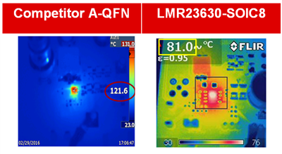
Additionally, the SOIC-8 on the LMR236xx family includes a single die attach pin (DAP) on the bottom to help extract the heat. This enables a lower junction-to-ambient thermal resistance (theta J/A) and better thermal performance than many QFN-style packages, like competitor A’s package in Figure 1.
 Figure 1 Thermal Images Taken at
vIN = 12V, vOUT = 5A at 3A, 2MHz
Figure 1 Thermal Images Taken at
vIN = 12V, vOUT = 5A at 3A, 2MHzFor many customers, the easy-to-use aspects of a package with pins outweigh the size advantages of a leadless package. Whether you prefer to stay on the cutting edge of package technology or want peace of mind from using a trusted and reliable package, the SIMPLE SWITCHER regulator family has an option for you. Check our website for more information about the SIMPLE SWITCHER LMR23610/25/35 family.
IMPORTANT NOTICE AND DISCLAIMER
TI PROVIDES TECHNICAL AND RELIABILITY DATA (INCLUDING DATASHEETS), DESIGN RESOURCES (INCLUDING REFERENCE DESIGNS), APPLICATION OR OTHER DESIGN ADVICE, WEB TOOLS, SAFETY INFORMATION, AND OTHER RESOURCES “AS IS” AND WITH ALL FAULTS, AND DISCLAIMS ALL WARRANTIES, EXPRESS AND IMPLIED, INCLUDING WITHOUT LIMITATION ANY IMPLIED WARRANTIES OF MERCHANTABILITY, FITNESS FOR A PARTICULAR PURPOSE OR NON-INFRINGEMENT OF THIRD PARTY INTELLECTUAL PROPERTY RIGHTS.
These resources are intended for skilled developers designing with TI products. You are solely responsible for (1) selecting the appropriate TI products for your application, (2) designing, validating and testing your application, and (3) ensuring your application meets applicable standards, and any other safety, security, or other requirements. These resources are subject to change without notice. TI grants you permission to use these resources only for development of an application that uses the TI products described in the resource. Other reproduction and display of these resources is prohibited. No license is granted to any other TI intellectual property right or to any third party intellectual property right. TI disclaims responsibility for, and you will fully indemnify TI and its representatives against, any claims, damages, costs, losses, and liabilities arising out of your use of these resources.
TI’s products are provided subject to TI’s Terms of Sale (www.ti.com/legal/termsofsale.html) or other applicable terms available either on ti.com or provided in conjunction with such TI products. TI’s provision of these resources does not expand or otherwise alter TI’s applicable warranties or warranty disclaimers for TI products.
Mailing Address: Texas Instruments, Post Office Box 655303, Dallas, Texas 75265
Copyright © 2023, Texas Instruments Incorporated