-
FemtoFET MOSFETs: Small as Sand but It’s All about That Pitch SSZTB60 June 2016 CSD15380F3 , CSD23280F3 , CSD25480F3
-
FemtoFET MOSFETs: Small as Sand but It’s All about That Pitch
FemtoFET MOSFETs: Small as Sand but It’s All about That Pitch
Kevin O'Connell
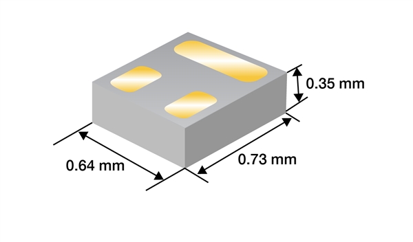
What contains more silicon: a grain of sand or TI’s latest FemtoFET product? As I sit in my beach chair watching the waves of the Atlantic roll onto the Jersey shore, my mind drifts over this question. The newly released F3 FemtoFETs, boasting a miniscule body size of 0.6mm by 0.7mm by 0.35mm (see Figure 1), can easily rival the grains of sand blowing under the Atlantic City boardwalk.
 Figure 1 F3 FemtoFET package
size.
Figure 1 F3 FemtoFET package
size.Check out the latest products to join the FemtoFET portfolio in the table below, including the ultra-low capacitance CSD15380F3.
| Part Number | N/P | Vds | Vgs | Id Cont. (A) | Typical Rdson (mohm) | Ciss (pF) | ||
|---|---|---|---|---|---|---|---|---|
| 4.5V | 2.5V | 1.8V | ||||||
| CSD15380F3 | N | 20 | 10 | 0.5 | 1170 | 2200 | x | 8.1 |
| CSD25480F3 | P | 20 | 12 | 1.7 | 132 | 203 | 420 | 119 |
| CSD23280F3 | P | 12 | 6 | 1.8 | 97 | 129 | 180 | 180 |
With devices this small, a critical consideration is the surface-mount technology (SMT) equipment used to attach the FemtoFETs to the board. The pitch of the device pads is the determining factor as to whether a customer’s SMT equipment can handle a package. Most high-volume personal electronics manufacturers have SMT equipment that can handle a minimum tolerance of 0.35mm pad pitch, but the SMT equipment at some industrial customers can only go down to a 0.50mm pad pitch.
The FemtoFET’s land grid array (LGA) package is similar to a silicon chip-scale package (CSP), except that the LGA has no attached solder balls. The gold-plated leads on the F3 FemtoFETs maintain the same 0.35mm pad pitch used on TI’s previous-generation F4 FemtoFETs. This enables existing F4 customers to use the smaller devices with full confidence that their SMT equipment can handle them.
In order to extend FemtoFETs into industrial applications, TI is also introducing a line of F5 FemtoFETs with a 0.50mm pitch, expanding the voltage range up to 60V. To learn more about this 60V F5 device, see my colleague Brett Barr’s blog post, “Shrink your industrial footprint with new 60V FemtoFET MOSFET.”
TI recommends Pb-free (SnAgCu) SAC alloy solder paste when board-mounting FemtoFETs such as the SAC305. You can use Type 3 paste, but the smaller-diameter Type 4 solder paste is preferable. The paste should be no-clean and water-soluble, although flux cleaning after board mount is still a good idea.
A stencil defines the locations where you should deposit the solder paste on the board. The thickness of the stencil and the x-y dimensions of the openings are important parameters. The maximum stencil thickness should be 100µm.
A wide variety of wearables and personal communication devices use low-leakage FemtoFETs. With gate and drain leakages typically in the single digit nano-amp range, FemtoFETs help to ensure that the battery charge of your personal electronics device lasts for the full day at the beach. With over 500 million FemtoFETs shipped since their introduction in 2013, as I relax on Long Beach Island this summer, I will be dreaming of all those pitch-perfect grains of sand. Get more information on TI’s family of FemtoFET MOSFETS.
Additional Resources
- Find additional stencil recommendations in the FemtoFET product data sheets.
- To read more about SMT and FemtoFETs, check out the FemtoFET Design Summary.
IMPORTANT NOTICE AND DISCLAIMER
TI PROVIDES TECHNICAL AND RELIABILITY DATA (INCLUDING DATASHEETS), DESIGN RESOURCES (INCLUDING REFERENCE DESIGNS), APPLICATION OR OTHER DESIGN ADVICE, WEB TOOLS, SAFETY INFORMATION, AND OTHER RESOURCES “AS IS” AND WITH ALL FAULTS, AND DISCLAIMS ALL WARRANTIES, EXPRESS AND IMPLIED, INCLUDING WITHOUT LIMITATION ANY IMPLIED WARRANTIES OF MERCHANTABILITY, FITNESS FOR A PARTICULAR PURPOSE OR NON-INFRINGEMENT OF THIRD PARTY INTELLECTUAL PROPERTY RIGHTS.
These resources are intended for skilled developers designing with TI products. You are solely responsible for (1) selecting the appropriate TI products for your application, (2) designing, validating and testing your application, and (3) ensuring your application meets applicable standards, and any other safety, security, or other requirements. These resources are subject to change without notice. TI grants you permission to use these resources only for development of an application that uses the TI products described in the resource. Other reproduction and display of these resources is prohibited. No license is granted to any other TI intellectual property right or to any third party intellectual property right. TI disclaims responsibility for, and you will fully indemnify TI and its representatives against, any claims, damages, costs, losses, and liabilities arising out of your use of these resources.
TI’s products are provided subject to TI’s Terms of Sale (www.ti.com/legal/termsofsale.html) or other applicable terms available either on ti.com or provided in conjunction with such TI products. TI’s provision of these resources does not expand or otherwise alter TI’s applicable warranties or warranty disclaimers for TI products.
Mailing Address: Texas Instruments, Post Office Box 655303, Dallas, Texas 75265
Copyright © 2023, Texas Instruments Incorporated