Optimizing LDO Voltage Accuracy
Whether it’s shooting darts or hitting a golf ball, accuracy matters. The same is true of a power supply –and it’s especially true when powering an ASIC, FPGA or any high-end processor. Simply put, the supply-voltage ranges of FPGAs and processors are becoming increasingly narrow.
Figure 1 is an example FPGA data sheet. The supply-voltage range for two supply rails, VCCINT and VCCBRAM, is 0.95V ±30mV for a particular model. That’s just slightly more than a ±3% tolerance. Making things worse, this voltage range shrinks when voltage monitoring and/or protection are introduced. As a result, the power supply could now be required to be 1% accurate or better to avoid a false trip.
 Figure 1 Recommended Operating
Conditions of an Example FPGA
Figure 1 Recommended Operating
Conditions of an Example FPGASuch limited range demands a correspondingly accurate power supply design. Although switched-mode power supplies are a typical choice for powering these loads, recent advancements have made low-dropout linear regulators (LDOs) attractive options as well. TI’s recently released TPS7A84 and TPS7A85 are 3A and 4A LDOs that combine high power supply rejection ratio (PSRR), low dropout and wide input-voltage ranges, making them ideal for minimizing voltage ripple. For this discussion, it’s the accuracy of these LDOs that make them compelling solutions to power FPGAs and processors. In this post, I’ll illustrate how to navigate the nuances of voltage-rail accuracy and how a performance LDO meets stringent accuracy requirements while minimizing total solution size and output capacitance.
DC Accuracy
In order to generate a voltage rail within the supply tolerance specified for a particular FPGA or processor, you must consider both the DC and AC output accuracy of the regulator. Of the two, it’s often easier to approximate DC accuracy. The main factors governing DC accuracy are:
- Variations in temperature.
- Variations in input voltage.
- Variations in load current.
- External resistor-divider tolerance.
Fortunately, the impact of these variations on accuracy (with the exception of external resistor-divider tolerances) is usually specified in the electrical characteristics table of a given voltage-regulator data sheet. Take the TPS7A85 datasheet. Output voltage accuracy is specified at a maximum of 1% when incorporating variations in load current, input voltage and temperature, as shown in Figure 2. (In fact, the output accuracy is even capable of reaching a maximum accuracy of 0.75% under certain conditions.) Characterizing accuracy in this way gives you an idea of the worst-case scenario.
 Figure 2 Output Voltage Accuracy of the TPS7A85
Of course, you can examine the relationship between these various factors and output accuracy independently. The electrical characteristics table and typical characteristics curves show individual specifications and plots for line and load regulation. Consulting these sections provides a better idea of how a particular set of conditions will affect output accuracy in an application.
External Resistors and ANY-OUT™ Operation
Although data-sheet accuracy specifications don’t incorporate external resistor-divider tolerances, they can still affect accuracy significantly. You can minimize the effect of such inaccuracy by either selecting tighter tolerance resistors (0.1% or less) or opting for a fixed-output voltage regulator (which has factory-trimmed, internal feedback resistors).
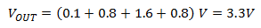
There is, however, a way to retain adjustability while also eliminating the compromised accuracy associated with external resistors. ANY-OUT operation allows you to set your desired output voltage by grounding a specific combination of ANY-OUT pins. Figure 3 shows an example of this operation where the TPS7A85 is programmed to output 3.3V by grounding the 100mV, 800mV and 1.6V pins.
 Figure 3 Using the TPS7A85’S ANY-OUT
Pins to Program the Output to 3.3V
Figure 3 Using the TPS7A85’S ANY-OUT
Pins to Program the Output to 3.3VAdding the values of these pins to the reference voltage (0.8V) gives a sum of 3.3V:
The benefit of ANY-OUT operation is that it allows you to adjust the output voltage without incurring inaccuracy stemming from external resistors. In other words, 1% accuracy is the worst-case scenario no matter how you program the output voltage. In fact, you can adjust the output voltage dynamically via the ANY-OUT pins. For more about this subject, see the application report, “ANY-OUT™ Low-Dropout Regulator Controlled by I2C IO Expander Device.”
AC Accuracy
AC accuracy also plays a large role in determining overall output accuracy. As with DC specifications, many FPGA and processor data sheets also specify maximum tolerable transient deviations from the normal supply range in terms of amplitude and duration. Dynamic shifts in LDO input voltage or load current can cause the output voltage to ring before the internal loop stabilizes. The amplitude and length of this ringing is contingent on a variety of factors, including internal topology, the input capacitor, the output capacitor and slew rate.
Load transient response is usually much more pronounced than that of line transients, especially when sourcing 3A or more. As such, the TPS7A85 data sheet details the load transient response under a variety of conditions. Figure 4 shows the load transient response as a function of output capacitance.
 Figure 4 Load Transient Response vs. Output Capacitance
As shown in Figure 4, increasing output capacitance helps dampen the amplitude of the ringing, which is necessary to prevent the output from deviating outside the permitted supply-voltage range of a given FPGA or processor. Of course, adding bulk output capacitance also takes up coveted space on a printed circuit board (PCB). The TPS7A84 and TPS7A85 ease this dilemma by having a wide-bandwidth control loop that responds quickly to dynamic load changes. As such, you can mute ringing with less output capacitance. The result is a solution size that is much more compact – the TPS7A85 is only 3.5mm by 3.5mm, after all.
Putting It All Together
Meeting the tight supply-voltage requirements of FPGAs and processors requires that you consider both DC and AC conditions. Performance LDOs have the ability to maintain DC accuracy of 1% or better across a variety of conditions. These LDOs also feature the excellent transient response necessary to subdue ringing associated with quick load changes. By combining these two advantages with the ability to filter switching noise, the TPS7A84 and TPS7A85 represent two solutions that can put your mind at rest when constructing a power scheme.
Be sure to subscribe to the Power House blog to receive more power management tips and insights.
IMPORTANT NOTICE AND DISCLAIMER
TI PROVIDES TECHNICAL AND RELIABILITY DATA (INCLUDING DATASHEETS), DESIGN RESOURCES (INCLUDING REFERENCE DESIGNS), APPLICATION OR OTHER DESIGN ADVICE, WEB TOOLS, SAFETY INFORMATION, AND OTHER RESOURCES “AS IS” AND WITH ALL FAULTS, AND DISCLAIMS ALL WARRANTIES, EXPRESS AND IMPLIED, INCLUDING WITHOUT LIMITATION ANY IMPLIED WARRANTIES OF MERCHANTABILITY, FITNESS FOR A PARTICULAR PURPOSE OR NON-INFRINGEMENT OF THIRD PARTY INTELLECTUAL PROPERTY RIGHTS.
These resources are intended for skilled developers designing with TI products. You are solely responsible for (1) selecting the appropriate TI products for your application, (2) designing, validating and testing your application, and (3) ensuring your application meets applicable standards, and any other safety, security, or other requirements. These resources are subject to change without notice. TI grants you permission to use these resources only for development of an application that uses the TI products described in the resource. Other reproduction and display of these resources is prohibited. No license is granted to any other TI intellectual property right or to any third party intellectual property right. TI disclaims responsibility for, and you will fully indemnify TI and its representatives against, any claims, damages, costs, losses, and liabilities arising out of your use of these resources.
TI’s products are provided subject to TI’s Terms of Sale (www.ti.com/legal/termsofsale.html) or other applicable terms available either on ti.com or provided in conjunction with such TI products. TI’s provision of these resources does not expand or otherwise alter TI’s applicable warranties or warranty disclaimers for TI products.
Mailing Address: Texas Instruments, Post Office Box 655303, Dallas, Texas 75265
Copyright © 2023, Texas Instruments Incorporated