-
How to Protect CAN Bus Transceivers from ESD and Transients
How to Protect CAN Bus Transceivers from ESD and Transients
Michael Peffers
Industrial networks such as controller area network (CAN), RS-485, RS-422, RS-232 and Profibus should be able to withstand harsh system-level transients (from electrostatic discharge [ESD] during handling, interruption of inductive loads, relay contact bounce and/or lightning strikes) in their end applications. Designing to meet these requirements can be challenging without the proper tools and knowledge about the standards that the design requires. In this post, I’ll discuss the International Electrotechnical Commission (IEC) 61000-4-2 ESD standard, an IEC 61000-4-2 ESD test setup and a transient voltage suppressor (TVS) diode circuit that helps protect your CAN transceiver.
The IEC 61000-4-2 ESD immunity test is a system-level ESD test that imitates a charged operator discharging onto an end system. The characteristics of the IEC ESD test differ from that of other ESD standards in rise times, the amount of energy delivered during the strike and the number of strikes administered during testing. Two types of testing methods are involved with the IEC ESD standard: contact discharge and air discharge. The contact ESD test discharges an ESD pulse from an IEC ESD gun directly onto the device under test (DUT). The air ESD discharge test involves moving the charged ESD gun toward the DUT until the air breaks down enough to allow conduction of an ESD strike between the ESD gun and the DUT. IEC ESD testing includes both positive and negative polarities, and a passing score is not possible unless both polarities at a single level survive. Figure 1 shows the IEC 61000-4-2 ESD test voltage and peak current levels.
 Figure 1 IEC 61000-4-2 ESD Test Voltage
Levels
Figure 1 IEC 61000-4-2 ESD Test Voltage
Levels*An open level. Dedicated equipment has to specify the level. You may need special test equipment if higher voltages than those shown are specified.
Figure 2 depicts the basic shape of the IEC ESD pulse and the timing sequence of the test pulses.
 Figure 2 Current Waveform of IEC ESD
Pulse and Timing Sequence of Test
Figure 2 Current Waveform of IEC ESD
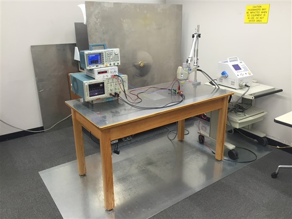
Pulse and Timing Sequence of TestFigure 3 shows the IEC ESD immunity-compliance test setup.
 Figure 3 IEC ESD-compliant Test
Setup
Figure 3 IEC ESD-compliant Test
SetupThe setup at Texas Instruments is fully compliant to the IEC ESD specification. The metal plate on the floor is connected directly to earth ground and separated from the top metal plane by two series 470kΩ resistors. On top of the upper ground plane is a thin insulator that keeps the DUT separated from the plane. This prevents the creation of a low-impedance path between the DUT and ground, enabling the DUT to absorb the full energy of the ESD strike. Lastly, the IEC ESD generator and gun are at the back right-hand corner of the table, both tied directly to earth ground. The IEC ESD gun has a discharge network made up of a 150pF capacitor and 330Ω resistor, which the standard specifies.
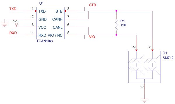
To protect a CAN transceiver against harsh transients such as the IEC 61000-4-2 ESD mentioned above, you can implement TVS diodes on bus lines CANH and CANL. The TVS diode acts as a clamping circuit to redirect any high-energy pulses to ground, away from the transceiver. When selecting a diode, keep in mind that the diode needs to be rated for the type of expected energy levels per the design requirements.
I paired TI’s TCAN1042 and TCAN1051 transceivers with the CDSOT23-SM712 bidirectional TVS diode, which is rated for IEC ESD applications and tested against the IEC ESD specification. Figure 4 shows the TCAN10xx transceiver with TVS diodes implemented, while Figure 5 and Figure 4 show the results from testing.
 Figure 4 TCAN10xx Transceiver with TVS
Protection
 Figure 5 TCAN10xx IEC ESD
Contact-discharge and Air-discharge Test Results
Figure 5 TCAN10xx IEC ESD
Contact-discharge and Air-discharge Test ResultsFor more information on the TCAN1042 and TCAN1051 with transient protection, please see the TI Designs IEC 61000 ESD, EFT and Surge Protected CAN Reference Design. Leave a comment below if you’d like to hear more about anything discussed in this post, or if there’s an interface topic you’d like to see in the future.
Additional Resources
- Download the TCAN1042 and TCAN1051 data sheets.
- Download the white paper, “Simplify CAN bus implementations with chokeless tranceivers”
- Check out these videos about EMC testing and the TCAN1042 and TCAN1051 CAN transceiver families:
IMPORTANT NOTICE AND DISCLAIMER
TI PROVIDES TECHNICAL AND RELIABILITY DATA (INCLUDING DATASHEETS), DESIGN RESOURCES (INCLUDING REFERENCE DESIGNS), APPLICATION OR OTHER DESIGN ADVICE, WEB TOOLS, SAFETY INFORMATION, AND OTHER RESOURCES “AS IS” AND WITH ALL FAULTS, AND DISCLAIMS ALL WARRANTIES, EXPRESS AND IMPLIED, INCLUDING WITHOUT LIMITATION ANY IMPLIED WARRANTIES OF MERCHANTABILITY, FITNESS FOR A PARTICULAR PURPOSE OR NON-INFRINGEMENT OF THIRD PARTY INTELLECTUAL PROPERTY RIGHTS.
These resources are intended for skilled developers designing with TI products. You are solely responsible for (1) selecting the appropriate TI products for your application, (2) designing, validating and testing your application, and (3) ensuring your application meets applicable standards, and any other safety, security, or other requirements. These resources are subject to change without notice. TI grants you permission to use these resources only for development of an application that uses the TI products described in the resource. Other reproduction and display of these resources is prohibited. No license is granted to any other TI intellectual property right or to any third party intellectual property right. TI disclaims responsibility for, and you will fully indemnify TI and its representatives against, any claims, damages, costs, losses, and liabilities arising out of your use of these resources.
TI’s products are provided subject to TI’s Terms of Sale (www.ti.com/legal/termsofsale.html) or other applicable terms available either on ti.com or provided in conjunction with such TI products. TI’s provision of these resources does not expand or otherwise alter TI’s applicable warranties or warranty disclaimers for TI products.
Mailing Address: Texas Instruments, Post Office Box 655303, Dallas, Texas 75265
Copyright © 2023, Texas Instruments Incorporated