-
The Value of Wettable Flank-plated QFN Packaging for Automotive Applications SSZTBN6 February 2016 LM53600-Q1 , LM53601-Q1
The Value of Wettable Flank-plated QFN Packaging for Automotive Applications
Murray Roose
To ensure that cars meet today’s demand for safety and high reliability, the automotive industry requires original equipment manufacturers (OEMs) to perform 100% automatic visual inspection (AVI) post-assembly. In the case of quad-flat no-lead (QFN) packages, there is no easily viewed solderable or exposed pins/terminals that enable you to determine whether or not the package successfully soldered on to the printed circuit board (PCB). The package edge has exposed copper for the terminals, these are prone to oxidation, making sidewall solder wetting difficult.
With QFN packages, sidewall solder coverage varies from 50-90%. OEMs must incur additional costs due to yield issues from false assembly failures, along with genuine fails where the assembly process has highlighted poor solder joints. The use of an X-ray machine to check for a good, reliable solder joint adds further expense or may not be available.
To resolve the issue of side lead wetting of leadless packaging for automotive and commercial component manufacturers, the wettable flank process was developed. This provides a visual indicator of solderability and lowers the inspection time. TI’s LM53600-Q1 and LM53601-Q1 automotive DC/DC buck regulators are available in a QFN package that uses a wettable flank process approved by many of the largest automotive OEMs.
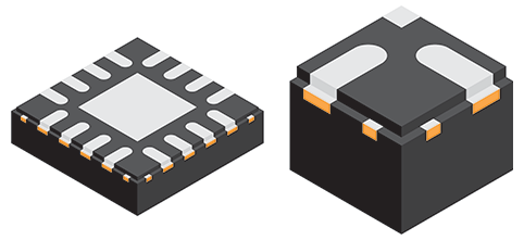
TI adopted special lead plating (SLP) as an additional step during the assembly process, where the package is step-cut and then re-plated with matte tin on half of the sidewall. See Figure 1 and Figure 2.
 Figure 1 Cross-section Comparison
between a Standard QFN and a Sawn-and-plated QFN with Wettable Flanks
 Figure 2 The Partial Cut and Re-plating
of Tin on the Half of the Sidewall of a QFN Package – Section Enlarged on
Right
Figure 2 The Partial Cut and Re-plating
of Tin on the Half of the Sidewall of a QFN Package – Section Enlarged on
RightTin plating provides a protective cover over the exposed copper. During the PCB assembly process, the solder joint will extend from the underside of the pad up the sidewall, resulting in an enhanced solder joint between the component and board. AVI can now assess the presence of a solder joint on all sides of the device. The presence of the side fillet indicates a higher probability of a complete joint, but can't guarantee this inspection at zero parts per million (PPM) without x-ray inspection. Solder de-wetting under the component can still occur due to poor paste block during the printing or PCB land oxidation, and this rate is best estimated as the de-wet PPM of the PCB lands for other non-QFN devices in the same assembly.
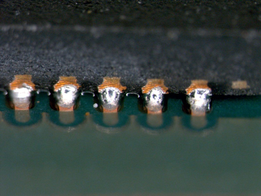
Figure 3 through Figure 6 highlight the solder joint between a QFN lead frame and a PCB with a clear exposed toe fillet, which assists with AVI and removes any false assembly failures.
 Figure 3 Standard QFN Package Side
View
 Figure 4 Toe Fillet on Standard
QFN
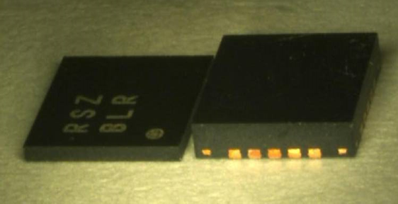
 Figure 5 Wettable Flank Lead Frame
Package Sidewall
 Figure 6 Toe Fillet on Wettable Flank
Lead Frame Package QFN
Figure 6 Toe Fillet on Wettable Flank
Lead Frame Package QFNIn summary, you can see that there is no difference in performance or quality with the wettable flank process. In this example, TI’s LM53600-Q1 and LM53601-Q1 automotive DC/DC buck regulators include a reliable solder joint and are able to pass the stringent 100% AVI requirements required by the automotive industry today.
IMPORTANT NOTICE AND DISCLAIMER
TI PROVIDES TECHNICAL AND RELIABILITY DATA (INCLUDING DATASHEETS), DESIGN RESOURCES (INCLUDING REFERENCE DESIGNS), APPLICATION OR OTHER DESIGN ADVICE, WEB TOOLS, SAFETY INFORMATION, AND OTHER RESOURCES “AS IS” AND WITH ALL FAULTS, AND DISCLAIMS ALL WARRANTIES, EXPRESS AND IMPLIED, INCLUDING WITHOUT LIMITATION ANY IMPLIED WARRANTIES OF MERCHANTABILITY, FITNESS FOR A PARTICULAR PURPOSE OR NON-INFRINGEMENT OF THIRD PARTY INTELLECTUAL PROPERTY RIGHTS.
These resources are intended for skilled developers designing with TI products. You are solely responsible for (1) selecting the appropriate TI products for your application, (2) designing, validating and testing your application, and (3) ensuring your application meets applicable standards, and any other safety, security, or other requirements. These resources are subject to change without notice. TI grants you permission to use these resources only for development of an application that uses the TI products described in the resource. Other reproduction and display of these resources is prohibited. No license is granted to any other TI intellectual property right or to any third party intellectual property right. TI disclaims responsibility for, and you will fully indemnify TI and its representatives against, any claims, damages, costs, losses, and liabilities arising out of your use of these resources.
TI’s products are provided subject to TI’s Terms of Sale (www.ti.com/legal/termsofsale.html) or other applicable terms available either on ti.com or provided in conjunction with such TI products. TI’s provision of these resources does not expand or otherwise alter TI’s applicable warranties or warranty disclaimers for TI products.
Mailing Address: Texas Instruments, Post Office Box 655303, Dallas, Texas 75265
Copyright © 2023, Texas Instruments Incorporated