-
A Simple Six-channel Power-rail Sequencing Solution
A Simple Six-channel Power-rail Sequencing Solution
Tim Reyes
Multichannel power-up and power-down sequencing has become a necessity in many power-supply systems. As the complexity of these systems increase, engineers must design for tighter timing specifications, power down in the reverse sequence, and handle a greater number of power rails.
The LM3880/LM3881 simple power-supply sequencer offers a simple and precise method to control the power-up and power-down sequencing of three independent power supplies – although with the complexity of power-supply systems today, three-channel sequencing may not be enough. So for systems that require sequencing more rails, you can cascade two LM3880/LM3881 devices for six-channel power sequencing. In this blog post, I’ll discuss how to cascade these devices for this application.
1 X LM3880 for Three-channel Sequencing
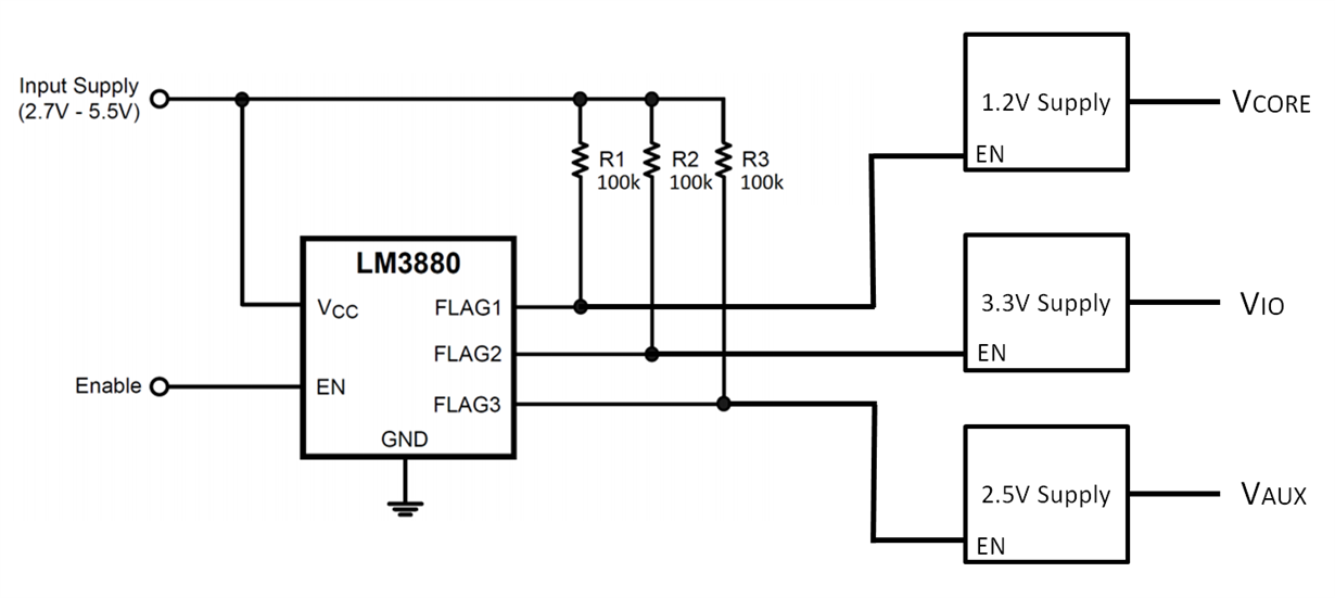
The LM3880 is typically used for power-up and power-down sequencing of three power supplies and provides a very simple solution with precise timing capability over a wide temperature range. This is especially important when the reverse sequence is required during power down, a requirement found in many microprocessors and field-programmable gate arrays (FPGAs). Figure 1 shows an example use of the LM3880 to correctly power-sequence the VCORE, VIO and VAUX rails of an FPGA in the correct order, both during power up and power down.
 Figure 1 Three-channel Power-supply Sequencing with the LM3880.
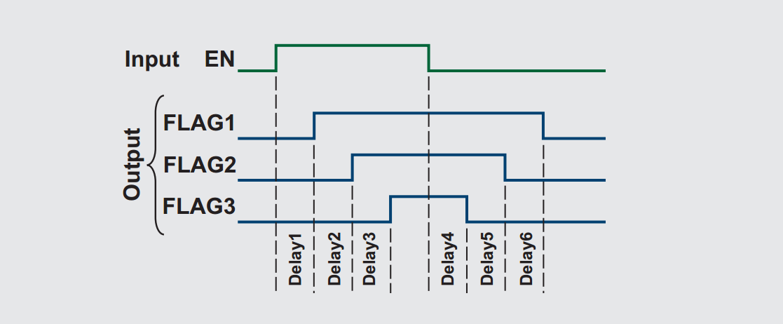
Figure 2 shows the timing diagram during power up and power down. In this example, the three FPGA supplies will be enabled starting with VCORE with 30ms of time in-between, and powered down in the reverse order, starting with VAUX. What engineers often overlook is that the reverse power-down order is just as important as the power-up order to prevent spurious current paths, for example, through internal P-N junctions of an FPGA. Therefore, proper sequencing will increase the longevity of the end product and improve product reliability.
 Figure 2 Three-channel Timing Diagram.
2 X LM3880 for Six-channel Sequencing
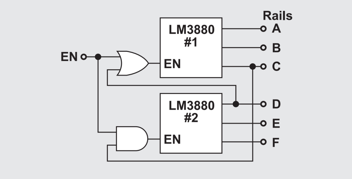
What about applications that require more than three rails? Is there a simple way to sequence these systems? Thankfully, there is! You can cascade two LM3880 integrated circuits (ICs) to enable six-channel power-up and power-down sequencing with only an external AND gate and OR gate. Figure 3 shows a simplified example of this, with the pull-up resistors omitted for simplicity.
 Figure 3 Six-channel Power-supply Sequencing with 2 X LM3880.
How Does the Cascading Scheme Work?
Upon power up, the OR gate ensures that LM3880 No. 1 is triggered with the EN rising edge and rails A, B and C begin powering up in order. The AND gate ensures that LM3880 No. 2 does not trigger until it has received both an EN signal and rail C has triggered.
On power down, the AND gate ensures that LM3880 No. 2 sees the EN falling edge and rails F, E and D powering down in order. The OR gate ensures that the first sequencer can’t see the EN falling edge until D has fallen.
Key Design Considerations for the Cascading Scheme
When deciding on the AND gate and OR gate, here are some key considerations:
-
The AND gate and OR gate outputs should be able to swing high enough and low enough such that the EN threshold of LM3880 can be triggered on both the rising and falling edge.
-
It is ideal to use the same supply for both LM3880 ICs, as well as the AND gate and OR gate.
-
The flag outputs of the LM3880 ICs must be able to trigger the AND gate and OR gate inputs on both the rising and falling edge. This means that when picking the AND gate and OR gate, you must consider their input thresholds and any hysteresis they have and ensure that the logic levels of the LM3880 flag outputs can trigger the input thresholds of the logic gates.
For the reasons I’ve mentioned, the LM3880 simple power-supply sequencer provides an easy-to-use and accurate solution to sequence up to six power-supply rails. With today’s very tight timing requirements and the need for reverse power-down sequencing, there is no simpler solution.
Additional Resources:
-
For a complete test report, which includes test waveforms and complete schematics, see the Simple 6-Channel Power Supply Sequencing Reference Design for Multi-rail Outputs TI Designs reference design, which highlights the use of the LM3880 for six-channel power sequencing.
- Quickly create a complete sequencer design with WEBENCH® Power Designer:
IMPORTANT NOTICE AND DISCLAIMER
TI PROVIDES TECHNICAL AND RELIABILITY DATA (INCLUDING DATASHEETS), DESIGN RESOURCES (INCLUDING REFERENCE DESIGNS), APPLICATION OR OTHER DESIGN ADVICE, WEB TOOLS, SAFETY INFORMATION, AND OTHER RESOURCES “AS IS” AND WITH ALL FAULTS, AND DISCLAIMS ALL WARRANTIES, EXPRESS AND IMPLIED, INCLUDING WITHOUT LIMITATION ANY IMPLIED WARRANTIES OF MERCHANTABILITY, FITNESS FOR A PARTICULAR PURPOSE OR NON-INFRINGEMENT OF THIRD PARTY INTELLECTUAL PROPERTY RIGHTS.
These resources are intended for skilled developers designing with TI products. You are solely responsible for (1) selecting the appropriate TI products for your application, (2) designing, validating and testing your application, and (3) ensuring your application meets applicable standards, and any other safety, security, or other requirements. These resources are subject to change without notice. TI grants you permission to use these resources only for development of an application that uses the TI products described in the resource. Other reproduction and display of these resources is prohibited. No license is granted to any other TI intellectual property right or to any third party intellectual property right. TI disclaims responsibility for, and you will fully indemnify TI and its representatives against, any claims, damages, costs, losses, and liabilities arising out of your use of these resources.
TI’s products are provided subject to TI’s Terms of Sale (www.ti.com/legal/termsofsale.html) or other applicable terms available either on ti.com or provided in conjunction with such TI products. TI’s provision of these resources does not expand or otherwise alter TI’s applicable warranties or warranty disclaimers for TI products.
Mailing Address: Texas Instruments, Post Office Box 655303, Dallas, Texas 75265
Copyright © 2023, Texas Instruments Incorporated