Power Tips: Synchronize Your SEPIC
A single-ended primary-inductor converter (SEPIC) does a great job of bucking or boosting the input voltage to maintain a regulated output voltage. This is useful in automotive applications or systems that may have multiple input sources available, but you don’t necessarily want to change the converter type. A SEPIC has many advantages, such as minimal active parts, and requires only a low-cost boost or flyback controller. However, like all topologies, it can also come up short in certain performance areas. One of these shortfalls is a limited maximum output current due to diode rectification. Let’s take a look at how synchronizing the output can help.
Figure 1 shows a basic SEPIC circuit, while Figure 2 details the corresponding key voltage and current waveforms. When Q2 turns on, it conducts the sum of the currents flowing in each winding of L1. This sum is equal to the input current plus Iout and reaches its maximum at full load and minimum input voltage. When Q2 turns off, these two currents are diverted through D1, into the output capacitor and load. Current only flows in D1 after Q2 is off because D1 is reversed-biased when Q2 is on.
 Figure 1 A Coupled-inductor SEPIC
Converter Has Two Current Paths
Figure 1 A Coupled-inductor SEPIC
Converter Has Two Current Paths SEPIC") Figure 2 Key Waveforms for a
Continuous-conduction-mode (CCM) SEPIC
Figure 2 Key Waveforms for a
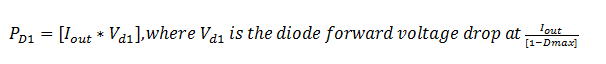
Continuous-conduction-mode (CCM) SEPICThe magnitude of the current flowing in D1 is Iout/(1-D), as shown in Figure 2. The conduction current may be significantly larger than Iout for input voltages much less than Vout, where the duty cycle becomes large. It’s easy to see that when operating at 50% duty cycle, where the input and output voltages are equal, the current in D1 is twice the output current. The average current in D1 is Iout, but to calculate the power dissipation in D1, it’s necessary to use the diode’s forward-voltage drop at the higher Iout/(1-D). This makes the maximum diode dissipation calculable by equation Equation 1:
Calculating the power dissipation with Iout/(1-D) may require the use of a diode with a higher current rating than anticipated, as well as a thermally enhanced package.
Figure 3 implements a synchronous SEPIC converter with an LM5122 sync-boost controller. It allows the use of an N-channel metal-oxide semiconductor field-effect transistor (MOSFET) (Q1) to replace diode D1, thereby reducing losses or allowing more output current for the same losses.
 Figure 3 A sync-SEPIC Converter
Implemented with a Sync-boost Controller and Floating-gate Drive Improves
Efficiency
Figure 3 A sync-SEPIC Converter
Implemented with a Sync-boost Controller and Floating-gate Drive Improves
EfficiencyA SEPIC has two switching nodes (TP2, TP3) rather than the single switching node of a boost. The gate of the SEPIC’s sync FET (Q1) cannot be directly connected to the boost controller’s high-side driver because its source (TP3) is not at the same potential as its SW pin (TP2). To drive it, I added a floating level-shifter circuit comprising R3/D2/C15. C15 has a voltage drop of VIN across it, which is the same voltage as the “flying” capacitor C1, providing the correct voltage swing across Q1 gate-to-source. R3/D2 restores the proper gate-drive offset (low = -0.5V, high = 7V).
To summarize, the rectifier losses in a SEPIC converter can impose a practical limit on the desired maximum output current because of thermal limitations. As the converter’s input voltage decreases, the diode’s conduction current increases, increasing losses, raising temperature, and hurting efficiency. By replacing the diode with a synchronous FET, it’s possible to reduce these losses. In the example circuit shown in Figure 3, the output current is increased by more than 1A over a traditional SEPIC with the same losses. Synchronous rectification obtains an efficiency greater than 95%.
For more about this topic, see this Power Tips article: “Three Ways to Boost Performance of a SEPIC.”
Additional Resources
- TI Designs reference PMP10886 REVA, “12V@5A Synchronous SEPIC Converter Reference Design.”
- Check out TI’s Power Tips blog series on Power House.
IMPORTANT NOTICE AND DISCLAIMER
TI PROVIDES TECHNICAL AND RELIABILITY DATA (INCLUDING DATASHEETS), DESIGN RESOURCES (INCLUDING REFERENCE DESIGNS), APPLICATION OR OTHER DESIGN ADVICE, WEB TOOLS, SAFETY INFORMATION, AND OTHER RESOURCES “AS IS” AND WITH ALL FAULTS, AND DISCLAIMS ALL WARRANTIES, EXPRESS AND IMPLIED, INCLUDING WITHOUT LIMITATION ANY IMPLIED WARRANTIES OF MERCHANTABILITY, FITNESS FOR A PARTICULAR PURPOSE OR NON-INFRINGEMENT OF THIRD PARTY INTELLECTUAL PROPERTY RIGHTS.
These resources are intended for skilled developers designing with TI products. You are solely responsible for (1) selecting the appropriate TI products for your application, (2) designing, validating and testing your application, and (3) ensuring your application meets applicable standards, and any other safety, security, or other requirements. These resources are subject to change without notice. TI grants you permission to use these resources only for development of an application that uses the TI products described in the resource. Other reproduction and display of these resources is prohibited. No license is granted to any other TI intellectual property right or to any third party intellectual property right. TI disclaims responsibility for, and you will fully indemnify TI and its representatives against, any claims, damages, costs, losses, and liabilities arising out of your use of these resources.
TI’s products are provided subject to TI’s Terms of Sale (www.ti.com/legal/termsofsale.html) or other applicable terms available either on ti.com or provided in conjunction with such TI products. TI’s provision of these resources does not expand or otherwise alter TI’s applicable warranties or warranty disclaimers for TI products.
Mailing Address: Texas Instruments, Post Office Box 655303, Dallas, Texas 75265
Copyright © 2023, Texas Instruments Incorporated