Snubbing the flyback converter
Robert Kollman
In October, we described how to snub the voltage across output rectifiers at turn on in the forward converter. Now, we look at snubbing the FET turn off voltage in the flyback converter.
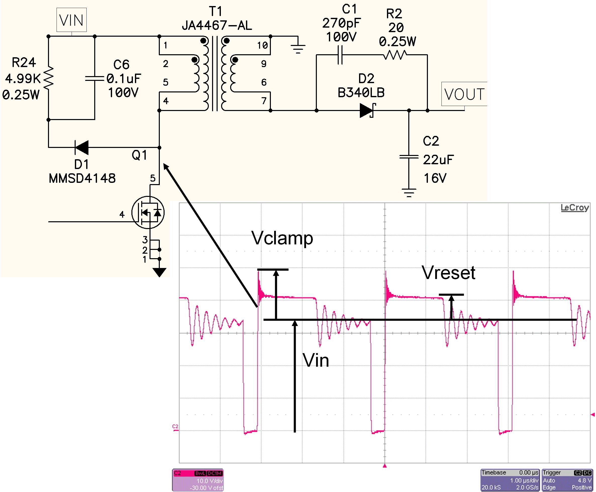
Figure 1 shows the flyback converter power stage and the primary MOSFET voltage waveform. This converter operates by storing energy in the primary inductance of a transformer and releasing the energy into the secondary when the MOSFET is turned off.
 Figure 1 Leakage inductance creates
excessive voltage at FET turn off.
Figure 1 Leakage inductance creates
excessive voltage at FET turn off.A snubber is often needed when the MOSFET is turned off as the transformer’s leakage inductance will cause the drain voltage to rise above the reflected output voltage (Vreset). The energy stored in the leakage inductance can avalanche the MOSFET, so a voltage clamping circuit comprising of D1, R24 and C6 is added. The clamp voltage on this circuit is set by the amount of energy in the leakage and the power dissipation in the resistor. A lower-value resistor will lower the clamp voltage, but will increase the power loss.
Figure 2 shows the transformer primary and secondary current waveforms.
 Figure 2 Leakage inductance steals the
output energy.
Figure 2 Leakage inductance steals the
output energy.On the left is the simplified power stage when the MOSFET is on. The input current ramps up through the series combination of leakage and mutual inductance. The right shows a simplified circuit during the off period. Here the voltage has reversed to the point that the output diode and clamp diode are forward biased. We show the output capacitor and diode reflected to the primary side of the transformer.
The two inductors are in series and are initially carrying the same current when Q1 turns off. That means that there is no current flow in the output diode D2 immediately after turn off and the total transformer current flows in D1. The voltage across the leakage inductance is the difference between the clamp and reset voltage and will tend to discharge the leakage rapidly.
As shown, it is a simple calculation to determine the energy diverted to the snubber. It turns out that you can reduce the diverted energy by reducing the time it takes to discharge the energy in the leakage inductance. This is accomplished by allowing the clamp voltage to increase.
Interestingly, you can calculate the trade-off between clamp voltage and snubber power dissipation. As shown in Figure 2, the power put into the clamp circuit is equal to the average clamp diode current times the clamp voltage (assuming a constant clamp voltage). Rearranging some terms we find the term ½ × F × L × I2, which relates to the output power of a discontinuous flyback converter. In this case, the inductance is the leakage inductance.
The expression is a little surprising in that the power loss is not just the energy stored in the leakage. It is always greater, but with a dependency on the clamp voltage. Figure 3 shows this relationship.
 Figure 3 Increasing the clamp voltage
reduces snubber loss.
Figure 3 Increasing the clamp voltage
reduces snubber loss.The graph plots the loss normalized to the leakage inductance energy loss versus the ratio of the clamp to reset voltage. At high values of clamp voltage, the snubber loss approaches the energy in the leakage inductance. As the clamp voltage is reduced by reducing the resistance, energy is diverted from the main output and the snubber dissipation increases dramatically. At a Vclamp/Vreset ratio of 1.5, it is almost three times the loss associated with the leakage inductance stored energy.
Coincidentally, the leakage inductance is often on the order of 1% of the magnetizing inductance. This makes Figure 3 even more interesting, in that it gives us an indication of the impact on efficiency that lowering the clamp voltage will have. The vertical axis then just becomes efficiency loss. So reducing the clamp ratio from 2 to 1.5 will have a one percent efficiency impact.
To summarize, the leakage inductance of a flyback converter can put an unacceptable voltage stress on the power switch. An RCD snubber can control the stress. However, there is a trade-off between the clamp voltage and circuit losses.
Previously published on EDN.com.
IMPORTANT NOTICE AND DISCLAIMER
TI PROVIDES TECHNICAL AND RELIABILITY DATA (INCLUDING DATASHEETS), DESIGN RESOURCES (INCLUDING REFERENCE DESIGNS), APPLICATION OR OTHER DESIGN ADVICE, WEB TOOLS, SAFETY INFORMATION, AND OTHER RESOURCES “AS IS” AND WITH ALL FAULTS, AND DISCLAIMS ALL WARRANTIES, EXPRESS AND IMPLIED, INCLUDING WITHOUT LIMITATION ANY IMPLIED WARRANTIES OF MERCHANTABILITY, FITNESS FOR A PARTICULAR PURPOSE OR NON-INFRINGEMENT OF THIRD PARTY INTELLECTUAL PROPERTY RIGHTS.
These resources are intended for skilled developers designing with TI products. You are solely responsible for (1) selecting the appropriate TI products for your application, (2) designing, validating and testing your application, and (3) ensuring your application meets applicable standards, and any other safety, security, or other requirements. These resources are subject to change without notice. TI grants you permission to use these resources only for development of an application that uses the TI products described in the resource. Other reproduction and display of these resources is prohibited. No license is granted to any other TI intellectual property right or to any third party intellectual property right. TI disclaims responsibility for, and you will fully indemnify TI and its representatives against, any claims, damages, costs, losses, and liabilities arising out of your use of these resources.
TI’s products are provided subject to TI’s Terms of Sale (www.ti.com/legal/termsofsale.html) or other applicable terms available either on ti.com or provided in conjunction with such TI products. TI’s provision of these resources does not expand or otherwise alter TI’s applicable warranties or warranty disclaimers for TI products.
Mailing Address: Texas Instruments, Post Office Box 655303, Dallas, Texas 75265
Copyright © 2024, Texas Instruments Incorporated