-
Design Considerations for CC1312PSIP FCC and IC Certified RF Module
Design Considerations for CC1312PSIP FCC and IC Certified RF Module
Abstract
This application note shows how to re-use the CC1312PSIP FCC Modular Certification. The Federal Communications Commission (FCC) and Industry Canada (IC) certification covers the frequency band of 902MHz to 928MHz, but the CC1312PSIP can also operate in the 863MHz to 876MHz ISM band. To re-use the FCC and IC Certification, you must verify that you use the certified software PHYs and copy the hardware reference design as much as possible.
The software section covers all of the various PHYs that have been tested and the maximum power that can be transmitted for each particular PHY. Several PHYs are supported and the benefits of each particular PHY are covered.
The hardware section covers the recommended layouts for a two-layer design and a four-layer design. There are differences between certified antennas and non-certified antennas in the requirements for the reuse of the modular approval for use in Canada and the United States. The last section covers the recommended testing of the CC1312PSIP when assembled onto a main board.
This document walks through software and hardware related questions and how to re-use the FCC or IC certification that enables a quicker time-to-market.
Trademarks
SimpleLink™ is a trademark of Texas Instruments.
Wi-Fi™ is a trademark of Wi-Fi Alliance.
Zigbee™ is a trademark of ZigBee Alliance.
Wi-SUN® is a registered trademark of Wi-SUN Alliance.
Arm® and Cortex® are registered trademarks of Arm Limited (or its subsidiaries) in the US and/or elsewhere.
Bluetooth® is a registered trademark of Bluetooth SIG, Inc.
All trademarks are the property of their respective owners.
1 Introduction
The SimpleLink™ CC1312PSIP [4.1] device is an RF certified System-in-Package (SiP) Sub-1GHz wireless module supporting Wi-SUN®, Wireless M-Bus, IEEE 802.15.4, IPv6-enabled smart objects (6LoWPAN), mioty, proprietary systems, including the TI 15.4-Stack. The CC1312PSIP microcontroller (MCU) is based on an Arm® Cortex® M4F main processor and optimized for low-power wireless communication and advanced sensing in grid infrastructure, building automation, retail automation, and medical applications.
The CC1312PSIP [4.1] has a low sleep current of 0.9μA with RTC and 80KB RAM retention. In addition to the main Cortex® M4F processor, the device also has an autonomous ultra-low power Sensor Controller CPU with fast wake-up capability. As an example, the sensor controller is capable of 1Hz ADC sampling at average 1μA system current.
The CC1312PSIP [4.1] has low soft error rate (SER) failure-in-time (FIT) for long operational lifetime. Always-on SRAM parity minimizes risk for corruption due to potential radiation events. Consistent with many customers 10 to 15 years or longer life cycle requirements, TI has a product life cycle policy with a commitment to product longevity and continuity of supply including dual sourcing of key components in the SIP.
The CC1312PSIP [4.1] device is part of the SimpleLink MCU platform, which consists of Wi-Fi™, Bluetooth® Low Energy, Thread, Zigbee™, Wi-SUN, Amazon Sidewalk, mioty, Sub-1GHz MCUs, and host MCUs. CC1312PSIP [4.1] is part of a portfolio that includes pin-compatible 2.4GHz SIPs for easy adaption of a wireless product to multiple communication standards. The common SimpleLink Low Power F2 SDK and SysConfig system configuration tool supports migration between devices in the portfolio. A comprehensive number of software stacks, application examples and SimpleLink Academy training sessions are included in the SDK.
By utilizing 3D assembly packaging with the SMD components placed on the CC1312PSIP [4.1] laminate and then placing the chip die directly above, the package volume is fully utilized. For the CC1312PSIP block diagram, see Figure 1-1. The RF filtering section has been was reduced to two singular components from 25 components by making two Integrated Passive Components (IPC). One IPC for the 14dBm Tx / Rx port and another for the 20dBm Tx port. This resulted in a final package size of 7 x 7mm with all components fully integrated.
 Figure 1-1 CC1312PSIP Block Diagram
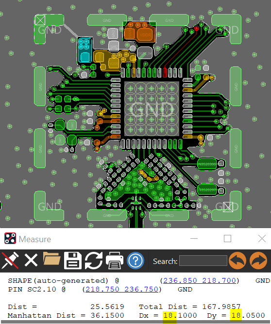
 Figure 1-2 Traditional Design With a QFN
Chipset
Figure 1-2 Traditional Design With a QFN
ChipsetWith the traditional design shown in Figure 1-2, this has a PCB floor space of approximately 324mm (18 x 18mm); with the CC1312PSIP [4.1] this was reduced to just 49mm (7 x 7mm). That is an 85 % size reduction.
In addition, to the size reduction, fully certified PHYs and FCC / IC modular certification that enables the option just to re-use the certification. There are also new features such as SW-TCXO that provide TCXO accuracy.