LaunchPad™ and Code Composer Studio™ are trademarks of Texas Instruments.
Bluetooth® is a registered trademark of Bluetooth SIG, Inc.
All trademarks are the property of their respective owners.
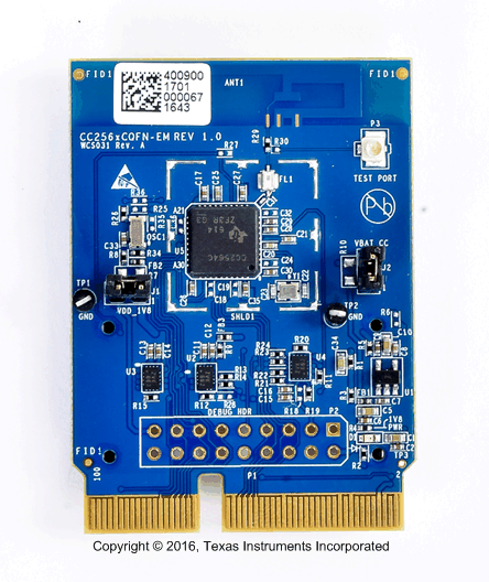
This user's guide is intended for use with TI's Bluetooth® development platform, the CC256xCQFN-EM board (see Figure 1-1). This guide helps users quickly get started integrating the board with TI's evaluation platforms and software SDKs. In addition, this user's guide describes the components and configurations of the board so that users can quickly get started using it for various Bluetooth applications.
This guide provides information about the module so that developers can use the board specifics to apply it to their applications. Module information and capabilities, including pin descriptions as well as available software and tools, enhance the user's out-of-box experience.
The following are example embedded wireless applications:
The CC256xC QFN EM board is the development environment for the CC256x family and plugs into TI's MSP432™ LaunchPad™ through the BOOST-CCEMADAPTER board.
This family is based on TI's CC256xC integrated circuit and uses a host controller interface (HCI), a cost-effective and flexible means for implementing a Bluetooth network. The HCI reduces BOM cost by eliminating redundant processing capacity and gives designers the flexibility to work with a controller of their choice, because the Bluetooth stack resides and executes on the host processor of the application. Figure 2-1 highlights various aspects of the CC256xCQFN-EM board.
The CC256xCQFN-EM board is intended for evaluation purposes and works with TI's Hardware Development Kit. For more information, see Section 6.
To help implement this reference design, schematics and layout files are available in the CC256XCQFN-EM Design Files.
The reference files including schematics, layout, and BOM for the CC256xCQFN-EM board can be found in the CC256XCQFN-EM Design Files.
Figure 3-1 shows a block diagram depicting the I/Os of the QFN board that are required for interfacing to the host controller. These I/Os can be interfaced to the host controller through either the COM connector or the RF1 and RF2 sockets.
For correct operation, ensure both jumpers are placed for connecting power to the device as follows in Table 3-1.
Jumper | Description |
---|---|
VBAT_CC | Main power supply for CC256xC |
VDD_1V8 | Supplies power to CC256xC I/Os |
These jumpers can also be used to measure the current consumption by placing current sense resistors on R10 for VBAT_CC and on R7 for VDD_1V8. Both these resistors are 0.10 Ω, 1/4 W. The VBAT_CC jumper can be used to to measure the voltage and power consumed by the CC256xC, including RF TX and RX while the VDD_IO jumper can be used to measure voltage and power consumed by the digital I/Os.
The board can be configured to route the RF output from the CC256xC to the onboard copper antenna or the onboard U.FL connector. This configuration is done by placing the resistor in either the R29 or R30 position which has negligible resistance of 0 Ω. R30 connects the RF to the U.FL while R29 connects to the copper antenna. The U.FL connector is used for conducted testing of the RF. The HCI Tester Tool can be used to test basic RF functionality on this board.
The RF1 and RF2 connectors can be sued to mount the TI MSP432 platform using the BOOST-CCEMADAPTER board. The RF I/Os are all at 3.3-V levels; this enables seamless integration of the host using TI's platforms that comes preinstalled with EM headers. Table 3-2 and Table 3-3 describe the standard pinout.
Pin No. | EM Adapter Pin Assignment | Pin No. | EM Adapter Pin Assignment |
---|---|---|---|
1 | GND | 2 | NC |
3 | MODULE_UART_CTS | 4 | NC |
5 | SLOW_CLK | 6 | NC |
7 | MODULE_UART_RX | 8 | NC |
9 | MODULE_UART_TX | 10 | NC |
11 | NC (not connected) | 12 | NC |
13 | NC | 14 | NC |
15 | NC | 16 | NC |
17 | NC | 18 | NC |
19 | GND | 20 | NC |
Pin No. | EM Adapter Pin Assignment | Pin No. | EM Adapter Pin Assignment |
---|---|---|---|
1 | NC | 2 | GND |
3 | NC | 4 | NC |
5 | NC | 6 | NC |
7 | 3.3V | 8 | MODULE_AUDIO_DATA_OUT |
9 | 3.3V | 10 | MODULE_AUDIO_DATA_IN |
11 | MODULE_AUDIO_FSYNC | 12 | NC |
13 | NC | 14 | NC |
15 | NC | 16 | NC |
17 | MODULE_AUDIO_CLK | 18 | MODULE_UART_RTS |
19 | WCS_NSHUTD | 20 | NC |
For complete evaluation of the audio applications while using the RF connectors (a.k.a. EM connectors), the level shifter U4 must be properly configured in order to ensure proper direction of PCM signals.
More information on the hardware changes required for PCM signals on EM connectors can be found in the CC256XCQFN-EM board design files (schematics and bill of materials).
The debug header is provided for testing and debugging purposes. The debug header exposes important signals used in the design such as power, ground, debug, UART, and audio signals. All I/Os are at 1.8V. Table 3-4 shows the pinout.
Pin No. | EM Adapter Pin Assignment | Pin No. | EM Adapter Pin Assignment |
---|---|---|---|
1 | GND | 2 | VBAT |
3 | VIO_HOST | 4 | GND |
5 | AUD_FSYNC_1V8 | 6 | AUD_CLK_1V8 |
7 | AUD_OUT_1V8 | 8 | AUD_IN_1V8 |
9 | CLK_REQ_OUT_1V8 | 10 | SLOW_CLK_EDGE |
11 | HCI_TX_1V8 | 12 | HCI_RX_1V8 |
13 | HCI_CTS_1V8 | 14 | HCI_RTS_1V8 |
15 | TX_DEBUG_1V8 | 16 | nSHUTDOWN_1V8 |
17 | VDD_1V8 | 18 | GND |
The COM connector, or edge card, is used to interface with TI's MPUs such as the AM437x and AM335x EVMs. As shown in Figure 3-3, the COM connector provides HCI, audio, slow clock, shutdown, and debug interfaces to the host connected through the edge card. All I/Os for the COM connector are at 1.8V. Some components must be DNI to use the COM connector. For more details, see the BOM.
Table 3-5 lists the COM card pinout.
Pin No. | Relevant COM Connector Pin Assignment |
---|---|
1 | SLOW_CLK_EDGE |
8 | 1V8_IN |
52 | AUD_CLK_1V8 |
54 | AUD_FSYNC_1V8 |
56 | AUD_IN_1V8 |
58 | AUD_OUT_1V8 |
66 | HCI_TX_1V8 |
68 | HCI_RX_1V8 |
70 | HCI_CTS_1V8 |
72 | HCI_RTS_1V8 |
76 | TX_DEBUG_1V8 |
89 | nSHUTDOWN_1V8 |
Pins 3, 9, 19, 37, 47, 63, 77, 83, 87, 95, and 97, as well as 2, 6, 18, 22, 42, 60, 64, and 92 are connected to ground.
All other pins are NC.
Some components must be removed (DNI) and R2 must be populated on the CC256XCQFN-EM to use the COM connector with the AM335x evaluation module (TMDXEVM3358) or similar Sitara EVM.
More information on the hardware changes required for the COM connector are in the CC256XCQFN-EM board design files (schematics and bill of materials).
The slow clock can come from two sources, internal and external to the board. The CC256xCQFN-EM has the option to place the slow clock on the board or source it from an external source. The source is connected to the SLOW_CLK_IN (see Figure 3-5) and can be a digital signal in the range of 0 to 1.8V.
The frequency accuracy of the slow clock must be 32.768kHz and ±250ppm for Bluetooth use (according to the Bluetooth specification).
When the MSP432 Launchpad is connected, the SLOW_CLK_IN signal, is sourced from the oscillator on the CC256xCQFN-EM board, therefore no additional clock source is needed.
Table 4-1 lists the module dimensions.
No. | Item | Dimension (in) | Tolerance | Remark |
---|---|---|---|---|
1 | Width | 1.550 | ± 0.001 | Smaller at COM end |
2 | Length | 2.125 | ± 0.001 | — |
3 | Height | 0.062 | ± 0.001 | — |
The Bluetooth software-based solution is based on TI's Bluetooth stack, such as the CC2564CMSP432BTBLESW. Detailed documentation is in the previous SDK.
TI supports the MSP432 LaunchPad (MSP-EXP432P401R).
In addition, a software development environment, for example Code Composer Studio™, is required. For a detailed description on use of these tools, see the HCI Tester Tool. Evaluation kits and modules are available through TI's network of authorized distributors.
Figure 5-1 shows the CC256xCQFN-EM board mounted to the MSP-EXP432P401R using the BOOST-CCEMADAPTER board, which uses the RF1 and RF2 interface board.
The HCI Tester Tool can be downloaded as a complete package from TI. This program is an intuitive, user-friendly tool to test TI's Bluetooth chips including this CC256xCQFN-EM board. More specifically, the program is used to measure RF performance of TI's Bluetooth chips.
Certifications for the CC256xCQFN-EM board include the CE Mark - Conformité Européenne. The CC256xC is also in the process of being certified as a Bluetooth controller subsystem by Bluetooth SIG (Special Interest Group).
Changes from Revision B (November 2016) to Revision C (January 2025)
TI PROVIDES TECHNICAL AND RELIABILITY DATA (INCLUDING DATASHEETS), DESIGN RESOURCES (INCLUDING REFERENCE DESIGNS), APPLICATION OR OTHER DESIGN ADVICE, WEB TOOLS, SAFETY INFORMATION, AND OTHER RESOURCES “AS IS” AND WITH ALL FAULTS, AND DISCLAIMS ALL WARRANTIES, EXPRESS AND IMPLIED, INCLUDING WITHOUT LIMITATION ANY IMPLIED WARRANTIES OF MERCHANTABILITY, FITNESS FOR A PARTICULAR PURPOSE OR NON-INFRINGEMENT OF THIRD PARTY INTELLECTUAL PROPERTY RIGHTS.
These resources are intended for skilled developers designing with TI products. You are solely responsible for (1) selecting the appropriate TI products for your application, (2) designing, validating and testing your application, and (3) ensuring your application meets applicable standards, and any other safety, security, or other requirements. These resources are subject to change without notice. TI grants you permission to use these resources only for development of an application that uses the TI products described in the resource. Other reproduction and display of these resources is prohibited. No license is granted to any other TI intellectual property right or to any third party intellectual property right. TI disclaims responsibility for, and you will fully indemnify TI and its representatives against, any claims, damages, costs, losses, and liabilities arising out of your use of these resources.
TI’s products are provided subject to TI’s Terms of Sale (www.ti.com/legal/termsofsale.html) or other applicable terms available either on ti.com or provided in conjunction with such TI products. TI’s provision of these resources does not expand or otherwise alter TI’s applicable warranties or warranty disclaimers for TI products.
Mailing Address: Texas Instruments, Post Office Box 655303, Dallas, Texas 75265
Copyright © 2024, Texas Instruments Incorporated