TIDT012 February 2022
Description
This reference design converts a wide 85–480 VAC input to a pair or reinforced, isolated 12-V and 24-V outputs. The 12-V output is capable of 14-W loading and the 24-V output is capable of 2.4-W loading. This reference design uses UCC28730 as a PSR valley-switching flyback design. A Silicon-Carbide low-side FET is used to achieve high efficiencies while operating across a wide input range. A balancing cap on the secondary keeps the two outputs in close regulation regardless of loading conditions.
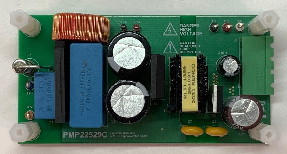
 Top Photo
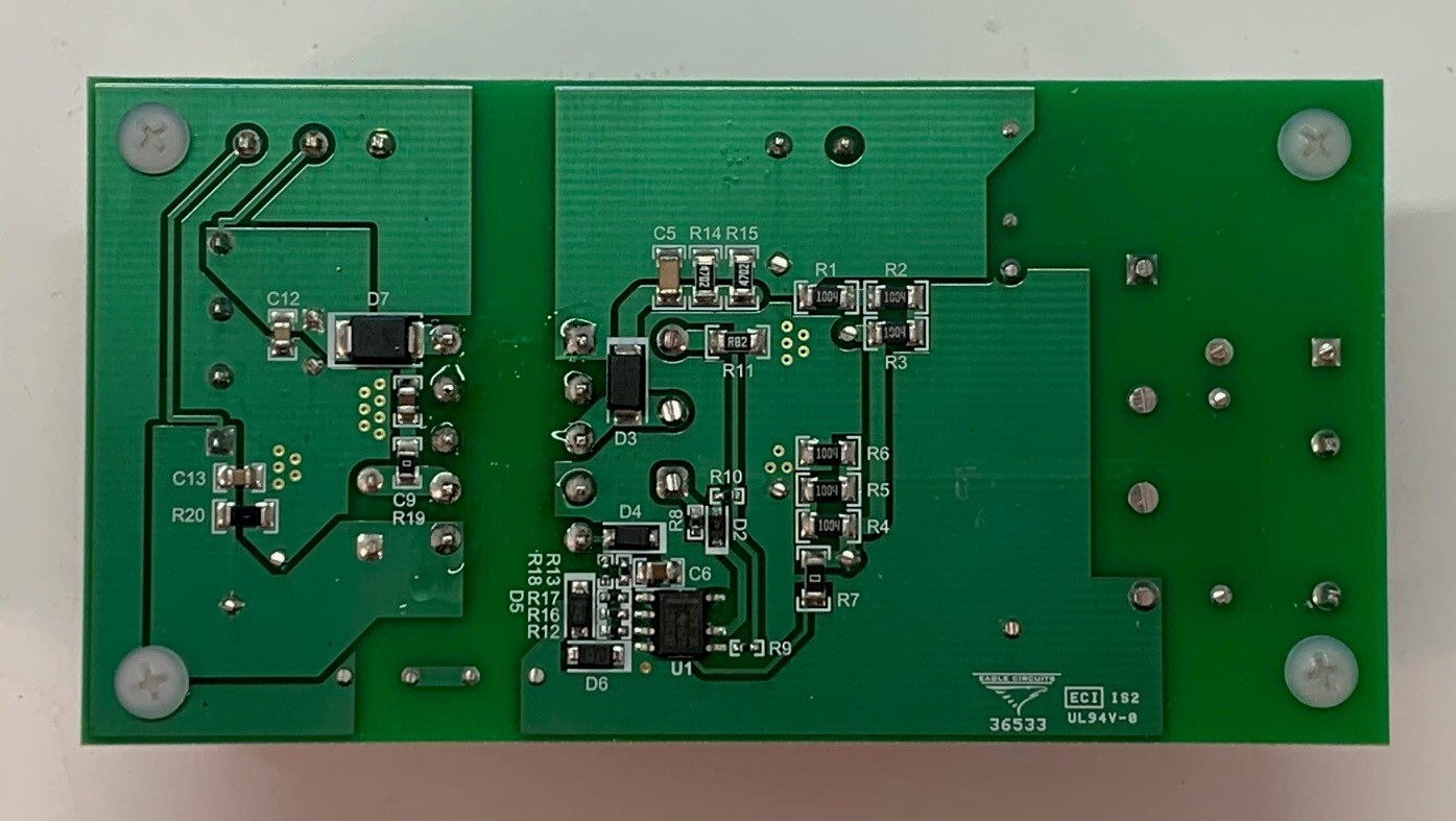
 Bottom Photo