-
Tiny Auxiliary SEPIC Converter Reference Design
Tiny Auxiliary SEPIC Converter Reference Design
Description
This reference design is a small SEPIC converter using the LM5158 device with integrated FET. The main design concern is using the smallest possible board space – setting the switching frequency to 2-MHz which means accepting some switching losses, accepting some magnetizing losses, but maintaining efficiency up to 400 mA at ≥ 80%.
Though the design has been tested up to 800-mA peak load, be aware that the continuous output is limited to 400 mA by thermal interface. Due to a pulsed load, the loop has been squeezed to the maximum bandwidth to enable the lowest output capacitance.
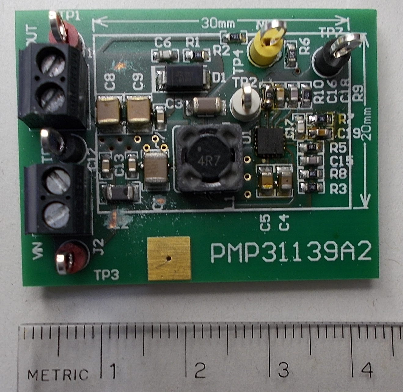
A small RF filter to prevent FM band noise is included, with a total solution size of 30 mm × 20 mm by using a two layer board, single side assembly, and a solid ground plane.
Features
- Tiny footprint, highly-integrated, ideal for space-constrained applications
- Small FM filter and dual random spectrum are for EMI mitigation
- The design is thoroughly tested
Applications
 Top Photo
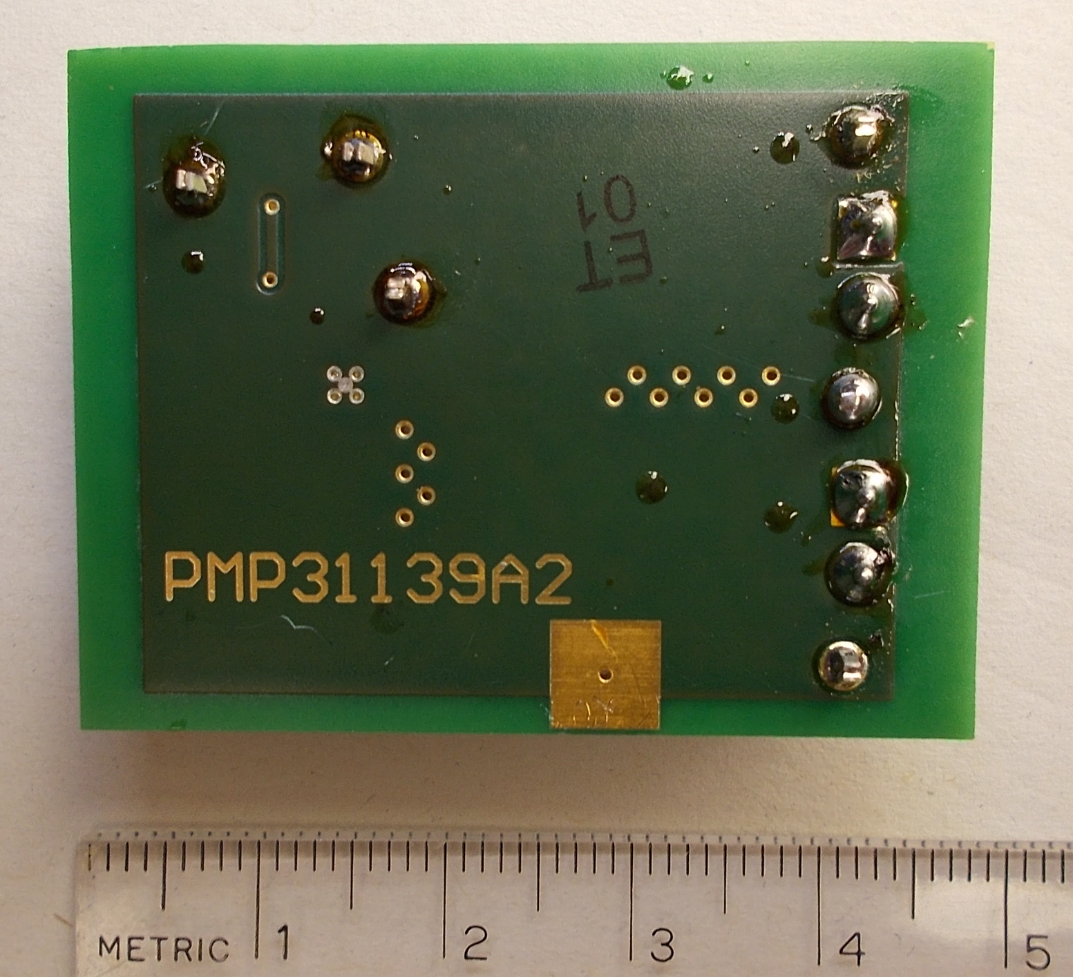
 Bottom Photo