-
4-Phase Buck 700-W Reference Design (Extended Input Voltage Range)
- Description
- Features
- Applications
- 1Test Prerequisites
- 2Testing and Results
- 3Waveforms for 2 × LM5143A-Q1 in Four Phase Configuration and Interleaved Operation
- A Individual Adjusting of the Rising Edge and Falling Edge With LM5143A
- B Measurements Across the Low-Side FETs to Check at All Four Phases
- C ON Demand – Assembly of Thermal Interface
- IMPORTANT NOTICE
4-Phase Buck 700-W Reference Design (Extended Input Voltage Range)
Description
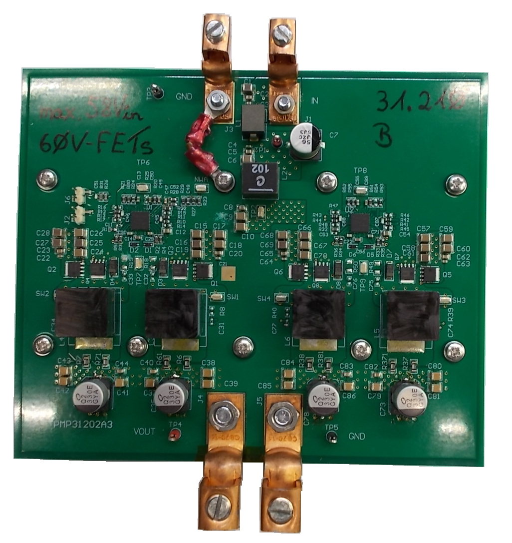
This reference design is a 700-W buck converter using the LM5143A-Q1 device. Due to lowest dead times, ultra-strong drivers, and the ability to adjust the rising edge and falling edge individually, the resulting efficiency is 98%.
Due to the reduced loss, the board area is also greatly reduced, now 150 mm × 125 mm, with a low profile of 12 mm or 15 mm, depending on the inductor selected.
Ample headroom for increased output power is available by using forced cooling or a heat sink mounted to a chassis. Using additional cooling options, the output current can be increased to 60-A continuous and higher.
The interleaved operation results in low root mean square (RMS) stress at the input capacitor and reduced ripple at the input and the output. A generic two stage EMI input filter is provided.
Features
- Power supply delivers up to 700-W continuous and up to 1-kW peak output power
- The interleaved four-phase buck topology provides ripple rejection
- The extended input range (compared to PMP31202) makes the design an excellent choice for truck applications
- This reference design is completely built and has completed testing in a lab
Applications
 Top
Photo