3.0-V to 15.2-V Input, 2-A, –1.8-V Inverting Power Module Reference Design for up to 125°C
Description
The TIDA-01405 design demonstrates an inverting power module (voltage inverter) to generate a –1.8-V rail at up to 2 A of current from a 3-V to 15.2-V input voltage. Such a negative voltage is required for many communications equipment systems as well as industrial equipment, such as test and measurement. Using the TPS82130 power module enables a very simple negative voltage inverter (inverting buck-boost) design to create a 1.8-V negative output voltage at high 2-A currents.
Resources
| TIDA-01405 | Design Folder |
| TPS82130 | Product Folder |

Features
- Simple Power Module Design
- Total Solution Size Less Than 50 mm2
- High Output Current of 2 A (VIN ≥ 5 V)
- Wide Input Voltage Range of 3 V to 15.2 V
- Low Noise (Less Than 10-mV Output Ripple)
- 125°C Rated Solution
1 System Overview
1.1 System Description
A negative voltage around –1.8 V is frequently required to bias the digital-to-analog (DAC) data converter in high-performance communications equipment systems, such as base stations and remote radio units. Data converters, such as the DAC38RF80 family of devices, require a negative voltage bias to power the current source array for the current sink output architecture. The 2 A of current provided in this reference design is sufficient to power multiple data converters in a single telecom system, which reduces the number of power supplies and their cost. The wide input voltage range supports many of the different supply voltages available in such systems. This enables the same design to be re-used for different systems which have different input voltages. The low noise and low output ripple enable a clean RF signal without distortion and does not limit the dynamic range of the data converter.
A negative voltage is also required in certain industrial applications, such as test and measurement, to power the same data converters. In addition, this negative voltage is useful for biasing operational amplifiers (op amps). In both applications, an integrated power module shortens the design time and enables a very-small solution size, while the low output noise has a minimal effect on the actual signal.
1.2 Key System Specifications
| PARAMETER | SPECIFICATIONS | DETAILS |
|---|---|---|
| Input voltage range (VIN) | 3 V to 15.2 V | — |
| Output voltage (VOUT) | –1.8 V | — |
| Output current (VIN ≥ 5 V) | 2 A | Figure 3-1 |
| Output current (VIN = 3 V) | 1 A | Figure 3-1 |
1.3 Highlighted Products
1.3.1 TPS82130
The TPS82130 is a 3-A, step-down converter power module, which integrates the power inductor to achieve a very-small solution size and simple design. The power module accepts up to a 17-V input voltage from its input pin to ground pin. This wide input voltage range is ideally suited for an inverting converter, which, at a minimum, requires a voltage rating of the input voltage plus the output voltage.
1.4 Design Considerations
1.4.1 Inverting Buck-Boost Topology Concept
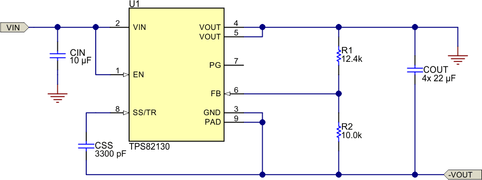
The inverting buck-boost topology is very similar to the buck topology. In the buck configuration that Figure 1-1 shows, the positive connection (VOUT) is connected to the VOUT pin of the power module and the return connection is connected to the ground (GND) of the power module. However, in the inverting buck-boost configuration that Figure 1-2 shows, the power module ground is used as the negative output voltage pin (labeled as –VOUT ). The terminal formerly known as the positive output in the buck configuration is used as the ground. This inverting topology allows the output voltage to be inverted and always lower than the ground.
 Figure 1-1 TPS82130 Buck Topology
 Figure 1-2 TPS82130 Inverting Buck-Boost Topology
The circuit operation is different in the inverting buck-boost topology than in the buck topology. Figure 1-3 (a) shows that the output voltage terminals are reversed, though the components are wired the same as a buck converter. As Figure 1-3 (b) shows, during the ON-time of the control MOSFET, the inductor is charged with current while the output capacitor supplies the load current. The inductor does not provide current to the load during this time. During the OFF-time of the control MOSFET and the ON-time of the synchronous MOSFET (see Figure 1-3 (c)), the inductor provides current to the load and the output capacitor. These changes affect many parameters, which the following subsections describe in further detail.
 Figure 1-3 Inverting
Buck-Boost Configuration
Figure 1-3 Inverting
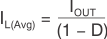
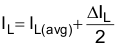
Buck-Boost ConfigurationThe average inductor current is affected in this topology. In the buck configuration, the average inductor current is equal to the average output current because the inductor always supplies current to the load during both the ON- and OFF-times of the control MOSFET. However, in the inverting buck-boost configuration, only the output capacitor supplies the load with current, while the load is completely disconnected from the inductor during the ON-time of the control MOSFET. During the OFF-time, the inductor connects to both the output capacitor and the load (see Figure 1-3). Because the OFF-time is 1 – D of the switching period, the average inductor current in Equation 1 is calculated as:
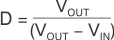
The duty cycle for the typical buck converter is simply VOUT / VIN, but the calculation of the duty cycle in Equation 2 for an inverting buck-boost converter becomes:
Equation 3 provides the peak-to-peak inductor ripple current:

where:
- ΔIL (A): Peak-to-peak inductor ripple current
- D: Duty cycle
- fS (MHz): Switching frequency
- L (µH): Inductor value of typically 1 µH
- VIN (V): Input voltage with respect to ground, not with respect to the device ground or VOUT.
Equation 4 calculates the maximum inductor current:
1.4.2 VIN and VOUT Range
The input voltage that can be applied to an integrated circuit (IC) operating in the inverting buck-boost topology is less than the input voltage for the same IC operating in the buck topology. The reason for this difference is because the ground pin of the IC is connected to the (negative) output voltage. Therefore, the input voltage across the device is VIN to VOUT, not VIN to ground. Thus, the input voltage range of the TPS82130 is 3 V to 17 V + VOUT, where VOUT is a negative value.
The output voltage range is the same as when configured as a buck converter, but negative. The output voltage for the inverting buck-boost topology must be set between –0.9 V and –6 V. The output voltage is set in the same way as the buck configuration, with two resistors connected to the FB pin. Use the same equation in the TPS82130 datasheet to set the output voltage, keeping both VOUT and VFB as positive values. The TIDA-01405 design sets the output voltage at –1.8 V, which gives an input voltage range of 3 V to 15.2 V.
1.4.3 Maximum Output Current
In the inverting buck-boost topology, the maximum output current is reduced as compared to the buck topology. This reduction is a result of the peak inductor current being higher, as calculated in Equation 4. With a power module, there are additional thermal limits arising from the small size of the power module itself. Finally, there are further limits on the maximum output current which occur from stability due to the right-half plane zero, which occurs in the inverting buck-boost topology. Figure 3-1 shows the maximum output current based on temperature rise and stability for the TIDA-01405 design. The current limit for the TPS82130 device occurs above all curves in Figure 3-1 and therefore does not limit the maximum output current more than thermal or stability limits. The current limit itself still operates to limit the peak inductor current.
1.4.3.1 Thermal Limits
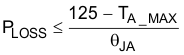
The primary maximum output current limitation in most designs is a thermal limitation. As the output current increases, the absolute power loss (in mW) in the TPS82130 also increases, which causes a higher temperature rise across the thermal impedance of the TPS82130 device.
The TPS82130 data sheet recommends operating below a device temperature of 110°C and forbids operating above 125°C for reliability. Therefore, Figure 3-1 contains two thermal limit lines: one for a 110°C and one for a 125°C operating temperature. These lines are calculated by multiplying the power loss of the TPS82130 from Figure 3-2 by the θJA of the TPS82130EVM-720, which is provided in the device data sheet as 46.1 °C/W, and adding this value to a 25°C ambient temperature.
Using this method, the maximum output current at any ambient temperature can be calculated. Simply subtract the maximum ambient temperature from either 110°C or 125°C to obtain the allowable temperature rise. Divide the θJA of the printed circuit board (PCB) by this temperature rise to obtain the allowable power loss. Find this power loss in Figure 3-2 to determine the maximum output current under specific conditions. 46.1°C/W is useful as an estimate of θJA. See Equation 5 for the calculation.
1.4.3.2 Stability Limits and Output Capacitor Selection
The 'Recommended' curve in Figure 3-1 shows the recommended maximum output current based on stability. The TIDA-01405 design should be operated at load currents below this line. In most applications, which have ambient temperatures above 25°C, the thermal limit lines move down below the 'Recommended' line (as explained in Section 1.4.3.1) and thus further limit the maximum output current.
The inverting buck-boost topology contains a right-half plane zero which significantly and negatively impacts the control loop response by adding an increase in gain along with a decrease in phase at a high frequency. This right-half plane zero can cause instability. Equation 6 estimates the frequency of the right-half plane zero.
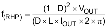
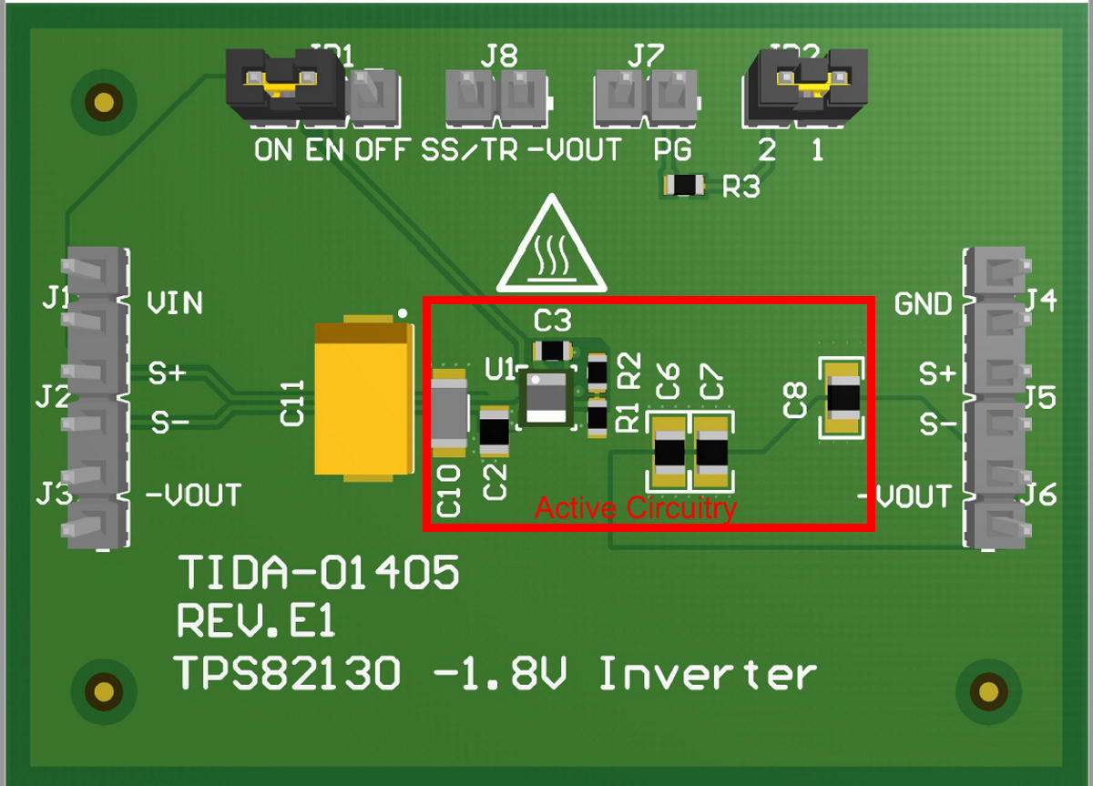
The TIDA-01405 design uses four 22-µF output capacitors, which have an effective capacitance of about 72 µF at the -1.8-V output voltage. This amount of capacitance pushes the crossover frequency of the control loop down to frequencies low enough so that the right-half plane zero is sufficiently higher in frequency for stability. While one of these output capacitors requires placement near the TPS82130 device, the others can be placed at the point of load and serve as their input decoupling capacitor. When three of the output capacitors are placed at the point of load, the solution size is below 50 mm2. If these three capacitors are included, the solution size of all components shown within the 'Active Circuitry' box on page 1 becomes around 75 mm2.
More output capacitance improves stability by increasing the separation between the right-half plane zero and crossover. The right-half plane zero frequency occurs at lower frequencies with lower input voltages, which have a higher duty cycle. Load transient testing is the best test for stability, as described in the Simplifying Stability Checks application report. Because the VOS pin of the TPS82130 is connected on the device, it is impossible to break the entire control loop and measure a bode plot.
1.4.4 Design Precautions
When using TPS82130 module for an inverting buck-boost application, there is a risk if the VIN and EN pins are connected together directly.
The inverting buck-boost is commonly used to power the negative side of a differential rail. If the positive rail is applied to this differential rail first, the downstream devices activate and their Iq charges a positive prebias voltage on the negative rail. Input brownout and quick power cycles are other scenarios that can prebias the negative rail and cause startup issues. With VIN and EN tied together, the device may enable before it has time to initialize internal circuitry which can cause unexpected startup behavior or cause the device to get stuck. Ensuring that the EN pin is asserted after VIN is powered on would eliminate this issue robustly.
There are three proposed workarounds to avoid this issue:
The first suggestion is to adjust the system power up sequence to prevent the unintended voltage buildup on the negative rail. This means enabling the negative rail first so that it is able to start up correctly, then enabling the positive rail. Adjusting the power on sequence this way will ensure that TPS82130 as inverting buck-boost converter has a correct startup.
If the application relies on the device enabling with VIN, then an RC filter is required to add a delay between VIN and EN pin. This ensures that the device has enough time to initialize the internal circuitry before the device is enabled to start regulating the output. The 100 kΩ and 1 μF RC filter provides the necessary delay between the VIN and EN pins for device's initialization. An example of this schematic modification is shown in two different options. One using a series resistor to limit the current into the EN pin Figure 1-4 and another using a schottky diode to clamp the EN pin Figure 1-5. When using the schottky diode option, the forward voltage drop should be selected less than 0.3 V so that the device doesn't exceed the absolute maximum rating on the EN pin.
Lastly, if the application requires enabling and disabling of the device from an external control signal, like a microcontroller or PG pin from an upstream device, then the order of power sequence is important. During power up, Vin must be applied before the EN signal and during power down, the EN pin should go low before Vin is removed. This ensures that EN pin does not exceed the maximum rating of VIN + 0.3 V, which can damage the device. See Section 1.4.5 for more information on level shifting the digital inputs.
1.4.5 Enable Pin Configuration
The device is enabled when the voltage at the EN pin trips its threshold and the input voltage is above the undervoltage lockout (UVLO) threshold. The TPS82130 device stops operation when the voltage on the EN pin falls below its threshold or the input voltage falls below the UVLO threshold.
Because VOUT is the IC ground in this configuration, the EN pin must be referenced to VOUT instead of ground. In the buck configuration, 0.9 V is considered as high and less than 0.3 V is considered as low. In the inverting buck-boost configuration, however, the VOUT voltage is the reference; therefore, the high threshold is 0.9 V + VOUT and the low threshold is 0.3 V + VOUT. For example, if VOUT = –1.8 V, then VEN is considered at a high level for voltages above –0.9 V and a low level for voltages below –1.5 V.
This behavior can cause difficulties enabling or disabling the part because, in some applications, the IC providing the EN signal may not be able to produce negative voltages. The level-shifter circuit that Figure 1-6 shows removes any difficulties associated with the offset EN threshold voltages by eliminating the requirement for negative EN signals. If disabling the TPS82130 is not desired, the EN pin may be directly connected to VIN without this circuit.

The positive signal that originally drove EN is instead tied to the gate of Q1 (SYS_EN). When Q1 is OFF (SYS_EN grounded), Q2 has 0 V across its VGS and also remains OFF. In this state, the EN pin is initially at the level of the output voltage (–1.8 V), which is below the low-level threshold, and disables the device.
When SYS_EN provides enough positive voltage to turn Q1 ON (VGS threshold as specified in the MOSFET datasheet), the gate of Q2 is at ground potential through Q1. This action drives the VGS of Q2 negative and turns Q2 ON. Then VIN ties to EN through Q2 and the pin is above the high-level threshold, which turns the device ON. Be careful to ensure that the VGD and VGS of Q2 remain within the MOSFET ratings during both the enabled and disabled states. Failing to adhere to this constraint can result in damaged MOSFETs.
Figure 3-17 and Figure 3-18 show the enable and disable sequence. The SYS_EN signal activates the enable circuit and the G/D node signal represents the shared node between Q1 and Q2. This circuit has been tested with a 3.3-V SYS_EN signal and dual N/PFET Si1029X. The EN signal is the output of the circuit and goes from VIN to VOUT to properly enable and disable the device. The PG pin is used as an output discharge to accelerate the return of VOUT to 0 V, when the IC is disabled.
1.4.6 Power Good Pin Configuration
The TPS82130 has a built-in power good (PG) function to indicate whether the output voltage has reached its appropriate level or not. The PG pin is an open-drain output that requires a pullup resistor. Because VOUT is the IC ground in this configuration, the PG pin is referenced to VOUT instead of ground, which means that the TPS82130 device pulls PG to VOUT when it is low.
This behavior can cause difficulties in reading the state of the PG pin, because in some applications the IC detecting the voltage level of the PG pin may not be able to withstand negative voltages. The level-shifter circuit shown in Figure 1-7 removes any difficulties associated with the offset PG pin voltages by eliminating the negative output signals of the PG pin. If the PG pin functionality is not required, it may be left floating or connected to VOUT without this circuit. Note that to avoid violating its absolute maximum rating, the PG pin should not be driven more than 6 V above the negative output voltage (IC ground).
 Figure 1-7 PG Pin Level Shifter
Inside the TPS82130, the PG pin is connected to an N-channel MOSFET (Q3). By tying the PG pin to the gate of Q1, when the PG pin is pulled low, Q1 is off and Q2 is on because Q2's VGS is at VCC. SYS_PG is then pulled to ground.
When Q3 turns OFF, the gate of Q1 is pulled to ground potential which turns Q1 ON. This sequence of events pulls the gate of Q2 below ground, which turns it OFF. SYS_PG is then pulled up to the VCC voltage. Note that the VCC voltage must be at an appropriate logic level for the circuitry connected to the SYS_PG net.
Figure 3-19 and Figure 3-20 show this PG pin level-shifter sequence. The PG signal activates the PG pin level-shifter circuit and the G/D node signal represents the shared node between Q1 and Q2. This circuit has been tested with a VCC of 5 V and dual NFET Si1902DL. The SYS_PG net is the output of the circuit and goes between ground and 5 V and is easily read by a separate device.
1.4.7 Discharging Output Voltage
If the TPS82130 device is disabled in a light-load or no-load condition, the PG pin can accelerate return of VOUT to 0 V by providing an additional discharge path. When the IC has been disabled through the EN pin, the PG pin is connected to the device ground (–VOUT) through an internal MOSFET. Placing a resistor between ground and the PG pin creates a discharge path to ground.
The added resistor must be sized to limit the current into the PG pin to a safe level, which the TPS82130 datasheet specifies as 10 mA maximum. A 200-Ω PG resistor has been chosen for this –1.8-V output voltage.
1.4.8 Input Capacitor Selection
An input capacitor, CIN, is required to provide a local bypass for the input voltage source. A low equivalent series resistance (ESR) X5R or X7R ceramic capacitor is best for input voltage filtering and minimizing interference with other circuits. For most applications, a 10-µF ceramic capacitor is recommended from VIN to ground (system ground, not –VOUT). The CIN capacitor value can be increased without any limit for better input voltage filtering.
For the inverting buck-boost configuration of the TPS82130, TI does not recommend to install a capacitor from VIN to –VOUT. Such a capacitor, if installed, provides an AC path from VIN to –VOUT. When VIN is applied to the circuit, this dV/dt across a capacitor from VIN to –VOUT creates a current that must return to ground (the return of the input supply) to complete its loop. This current may flow through the body diode of the internal low-side MOSFET and the inductor to return to ground. Flowing through the body diode pulls the VOUT pin below IC ground, which violates its absolute maximum rating. Such a condition may damage the TPS82130 and is not recommended; therefore, a capacitor from VIN to –VOUT is not required or recommended. If such a capacitor (CBP) is present, then a Schottky diode must be installed on the output, as the schematic in Figure 1-8 shows.
 Figure 1-8 Installation of Schottky Diode D1 Required, if Installing CBP
2 Getting Started Hardware
To test this TI Design, simply apply an input voltage between the J1 and J4 connectors. Then, connect a jumper between ON and EN on JP1.
3 Testing and Results
3.1 Test Results
 Figure 3-1 Maximum Output Current
 Figure 3-2 Efficiency Over Load
") Figure 3-3 Efficiency Over VIN (1-A Load)
Figure 3-3 Efficiency Over VIN (1-A Load) Figure 3-4 Load Regulation
") Figure 3-5 Line Regulation (1-A Load)
Figure 3-5 Line Regulation (1-A Load)") Figure 3-6 Switching Frequency Over VIN (1-A Load)
Figure 3-6 Switching Frequency Over VIN (1-A Load) Figure 3-7 Switching Frequency Over Load
") Figure 3-8 Transient Response (3.3 VIN, 0-A to 1-A Load Step)
Figure 3-8 Transient Response (3.3 VIN, 0-A to 1-A Load Step)") Figure 3-9 Transient Response (5 VIN, 0-A to 1-A Load Step)
Figure 3-9 Transient Response (5 VIN, 0-A to 1-A Load Step)") Figure 3-10 Transient Response (12 VIN, 0-A to 1-A Load Step)
Figure 3-10 Transient Response (12 VIN, 0-A to 1-A Load Step)") Figure 3-11 Output Voltage Ripple (3.3 VIN, 1-mA Load)
Figure 3-11 Output Voltage Ripple (3.3 VIN, 1-mA Load)") Figure 3-12 Output Voltage Ripple (3.3 VIN, 1-A Load)
Figure 3-12 Output Voltage Ripple (3.3 VIN, 1-A Load)") Figure 3-13 Output Voltage Ripple (5 VIN, 1-mA Load)
Figure 3-13 Output Voltage Ripple (5 VIN, 1-mA Load)") Figure 3-14 Output Voltage Ripple (5 VIN, 1-A Load)
Figure 3-14 Output Voltage Ripple (5 VIN, 1-A Load)") Figure 3-15 Output Voltage Ripple (12 VIN, 1-mA Load)
Figure 3-15 Output Voltage Ripple (12 VIN, 1-mA Load)") Figure 3-16 Output Voltage Ripple (12 VIN, 1-A Load)
Figure 3-16 Output Voltage Ripple (12 VIN, 1-A Load)") Figure 3-17 Start-up on EN (5 VIN, No Load)
Figure 3-17 Start-up on EN (5 VIN, No Load)") Figure 3-18 Shutdown on EN (5 VIN, No Load)
Figure 3-18 Shutdown on EN (5 VIN, No Load)") Figure 3-19 PG on Start-up (5 VIN, No Load)
Figure 3-19 PG on Start-up (5 VIN, No Load)") Figure 3-20 PG on Shutdown (5 VIN, No Load)
Figure 3-20 PG on Shutdown (5 VIN, No Load)4 Design Files
4.1 Schematics
To download the schematics, see the design files at TIDA-01405.
4.2 Bill of Materials
To download the bill of materials (BOM), see the design files at TIDA-01405.
4.3 PCB Layout Recommendations
4.3.1 Layout Prints
To download the layer plots, see the design files at TIDA-01405.
4.4 Gerber Files
To download the Gerber files, see the design files at TIDA-01405.
4.5 Assembly Drawings
To download the assembly drawings, see the design files at TIDA-01405.
5 Related Documentation
- Texas Instruments, Simplifying Stability Checks, application report.
- Texas Instruments, Using the TPS62125 in an Inverting Buck-Boost Topology, TPS62125 application report.
- Texas Instruments, TPS82130 17-V Input 3-A Step-Down Converter MicroSiP™ Module with Integrated Inductor, data sheet.
6 Trademarks
TI E2E™ is a trademark of Texas Instruments.
All trademarks are the property of their respective owners.
7 Revision History
Changes from Revision A (April 2017) to Revision B (January 2023)
- Updated the numbering format for tables, figures, and cross-references throughout the documentGo
- Added Design Precautions topic Go
Changes from Revision * (March 2017) to Revision A (April 2017)
- Updated arrangement of Section 1.5, Section 1.6, Section 1.7, and Section 1.8 to Section 1.4.5 , Section 1.4.6 , Section 1.4.7 , and Section 1.4.8 Go
- Updated Efficiency Over V_IN (1-A Load ) image replacing IOUT (mA) with the x-axis to VIN (V) Go
IMPORTANT NOTICE AND DISCLAIMER
TI PROVIDES TECHNICAL AND RELIABILITY DATA (INCLUDING DATASHEETS), DESIGN RESOURCES (INCLUDING REFERENCE DESIGNS), APPLICATION OR OTHER DESIGN ADVICE, WEB TOOLS, SAFETY INFORMATION, AND OTHER RESOURCES “AS IS” AND WITH ALL FAULTS, AND DISCLAIMS ALL WARRANTIES, EXPRESS AND IMPLIED, INCLUDING WITHOUT LIMITATION ANY IMPLIED WARRANTIES OF MERCHANTABILITY, FITNESS FOR A PARTICULAR PURPOSE OR NON-INFRINGEMENT OF THIRD PARTY INTELLECTUAL PROPERTY RIGHTS.
These resources are intended for skilled developers designing with TI products. You are solely responsible for (1) selecting the appropriate TI products for your application, (2) designing, validating and testing your application, and (3) ensuring your application meets applicable standards, and any other safety, security, or other requirements. These resources are subject to change without notice. TI grants you permission to use these resources only for development of an application that uses the TI products described in the resource. Other reproduction and display of these resources is prohibited. No license is granted to any other TI intellectual property right or to any third party intellectual property right. TI disclaims responsibility for, and you will fully indemnify TI and its representatives against, any claims, damages, costs, losses, and liabilities arising out of your use of these resources.
TI’s products are provided subject to TI’s Terms of Sale (www.ti.com/legal/termsofsale.html) or other applicable terms available either on ti.com or provided in conjunction with such TI products. TI’s provision of these resources does not expand or otherwise alter TI’s applicable warranties or warranty disclaimers for TI products.
Mailing Address: Texas Instruments, Post Office Box 655303, Dallas, Texas 75265
Copyright © 2023, Texas Instruments Incorporated