-
LM21305 3-V to 18-V, 5-A, Adjustable Frequency Synchronous Buck Converter
- 1 Features
- 2 Applications
- 3 Description
- 4 Revision History
- 5 Description (continued)
- 6 Pin Configuration and Functions
- 7 Specifications
-
8 Detailed Description
- 8.1 Overview
- 8.2 Functional Block Diagram
- 8.3
Feature Description
- 8.3.1 Synchronous DC-DC Switching Converter
- 8.3.2 Peak Current-Mode Control
- 8.3.3 Switching Frequency Setting and Synchronization
- 8.3.4 Light-Load Operation
- 8.3.5 Precision Enable
- 8.3.6 Device Enable, Soft-Start, and Pre-Bias Startup Capability
- 8.3.7 Peak Current Protection and Negative Current Limiting
- 8.3.8 PGOOD Indicator
- 8.3.9 Internal Bias Regulators
- 8.3.10 Minimum On-Time Considerations
- 8.4 Device Functional Modes
-
9 Application and Implementation
- 9.1 Application Information
- 9.2
Typical Application
- 9.2.1 Design Requirements
- 9.2.2
Detailed Design Procedure
- 9.2.2.1 Setting the Output Voltage
- 9.2.2.2 Calculating the Duty Cycle
- 9.2.2.3 Input Capacitors
- 9.2.2.4 AVIN Filter
- 9.2.2.5 Switching Frequency Selection
- 9.2.2.6 Filter Inductor
- 9.2.2.7 Output Capacitor
- 9.2.2.8 Efficiency Considerations
- 9.2.2.9 Load Current Derating When Duty Cycle Exceeds 50%
- 9.2.2.10 Control Loop Compensation
- 9.2.2.11 Compensation Components Selection
- 9.2.2.12 Plotting the Loop Gain
- 9.2.2.13 High Frequency Considerations
- 9.2.2.14 Bootstrap Capacitor
- 9.2.2.15 5V0 and 2V5 Capacitors
- 9.2.2.16 Maximum Ambient Temperature
- 9.2.3 Application Curves
- 10Power Supply Recommendations
- 11Layout
- 12Device and Documentation Support
- 13Mechanical, Packaging, and Orderable Information
- IMPORTANT NOTICE
Package Options
Mechanical Data (Package|Pins)
- RSG|28
Thermal pad, mechanical data (Package|Pins)
Orderable Information
LM21305 3-V to 18-V, 5-A, Adjustable Frequency Synchronous Buck Converter
1 Features
- High-Efficiency Synchronous DC-DC Converter:
- External Frequency Synchronization
- Accurate 0.598-V Feedback Voltage Reference
- Ultra-Fast Line and Load Transient Response:
- Peak Current-Mode Control
- Internal Slope Compensation
- High-Bandwidth Error Amplifier
- Ultra-Low Shutdown Quiescent Current
- Wide Duty-Cycle Operating Range:
- TON-MIN: 70 ns for Low VOUT
- TOFF-MIN: 50 ns for High Duty Cycle
- Diode Emulation Mode at Light Loads
- Integrated Bias Supply LDO Sub-Regulators
- Internal Soft-Start Function:
- Monotonic Startup into Pre-Biased Loads
- Precision Enable Input with Hysteresis
- Open-Drain PGOOD Indicator
- Internal Input Undervoltage Lockout (UVLO)
- Cycle-by-Cycle Overcurrent Protection
- Output Overvoltage Protection (OVP)
- Thermal Shutdown Protection with Hysteresis
- 5-mm x 5-mm WQFN-28 PowerPAD™ Package
2 Applications
- DC-DC Converters and POL Modules
- DSP and FPGA Core Voltage Supplies
- Telecommunications Infrastructure
- Embedded Computing, Servers, and Storage
3 Description
The LM21305 is a full-featured, 5-A, synchronous buck dc-dc converter optimized for solution size, flexibility, and high conversion efficiency. High-power density LM21305 designs are easily achieved by virtue of monolithic integration of high-side and low-side power MOSFETs, high switching frequency, peak current-mode control, and optimized thermal design. The efficiency of the LM21305 is maximized at light loads with diode emulation mode operation and at heavy loads by optimal design of the MOSFET adaptive gate drivers to minimize switch dead-times and body-diode conduction losses.
The LM21305 accepts a wide input voltage range of 3 V to 18 V for interface to various intermediate bus voltages, including 3.3-V, 5-V, and 12-V rails. A 1.5% voltage reference and 70-ns, high-side MOSFET minimum controllable on-time enable output voltages as low as 0.598 V with excellent setpoint accuracy. The LM21305 is available in a 5-mm × 5-mm2 WQFN-28 thermally-enhanced package with 0.5-mm pitch.
Device Information(1)
| PART NUMBER | PACKAGE | BODY SIZE (NOM) |
|---|---|---|
| LM21305 | WQFN (28) | 5.00 mm × 5.00 mm |
- For all available packages, see the orderable addendum at the end of the data sheet.
Typical Application Circuit

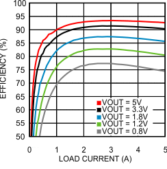
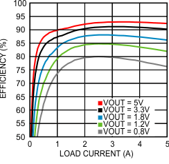
Typical Efficiency at 12 V, 500 kHz
4 Revision History
Changes from F Revision (March 2013) to G Revision
- Changed Features, Applications, and Description sections and page 1 graphicsGo
- Added Feature Description section, ESD Ratings table, Device Functional Modes section, Application and Implementation section, Power Supply Recommendations section, Layout section, Device and Documentation Support section, and Mechanical, Packaging, and Orderable Information section. Go
- Changed Precision Enable sectionGo
5 Description (continued)
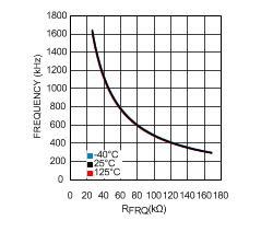
The LM21305 offers flexible system configuration with programmable switching frequency from 300 kHz to 1.5 MHz using one resistor or by external clock synchronization for beat-frequency-sensitive and multi-regulator applications. On-chip bias supply low-dropout (LDO) sub-regulators eliminate the need for an external bias power and simplify circuit board layout. The device also offers an internal soft-start to limit inrush current and provide monotonic startup capability into unbiased and pre-biased loads, integrated boot diodes, cycle-by-cycle current limiting, and thermal shutdown. Peak current-mode control with a high-gain error amplifier maintains stability throughout the entire input voltage and load current ranges, enabling excellent line and load transient response.
The LM21305 features internal output overvoltage protection (OVP) and overcurrent protection (OCP) circuits for increased system reliability. An integrated open-drain, PGOOD indicator provides output voltage monitoring, power-rail sequencing capability, and fault indication. Other features include thermal shutdown with automatic recovery, low PWM minimum on-time, low shutdown quiescent current, and precision enable with hysteresis for programmable line undervoltage lockout (UVLO).
6 Pin Configuration and Functions
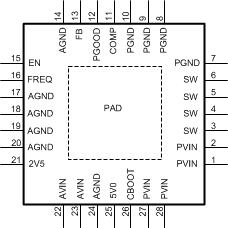
Pin Functions
| PIN | Type(1) | DESCRIPTION | |
|---|---|---|---|
| NAME | NO. | ||
| 2V5 | 21 | P | 2.5-V output of the internal LDO regulator. Bypass to AGND with a 0.1-µF ceramic capacitor. Loading this pin is not recommended. |
| 5V0 | 25 | P | 5.0-V output of the internal LDO regulator. Bypass to PGND with a 1-µF ceramic capacitor. Loading this pin is not recommended. |
| AGND | 14, 17–20, 24 | G | Analog ground for the internal bias circuitry and signal return connection for analog functions, including COMP network, frequency adjust resistor, and 2V5 decoupling capacitor. |
| AVIN | 22, 23 | P | Analog power input. AVIN powers the internal 2.5-V and 5.0-V LDOs that provide bias current and internal driver power, respectively. AVIN can be connected to PVIN through a low-pass RC filter or can be supplied by a separate rail. |
| CBOOT | 26 | P | High-side bootstrap connection to drive the high-side MOSFET. Connect a 100-nF bootstrap capacitor between the CBOOT and SW pins. |
| COMP | 11 | A | Compensation node. This pin is an output voltage control loop error amplifier output. Connect an external compensation network to ensure stability. |
| EN | 15 | I | Precision enable pin. Use an external divider to set the device turn-on threshold. If not used, connect the EN pin to AVIN. |
| FB | 13 | A | Voltage feedback pin. Connect this pin to the output voltage directly or through a resistor divider to set the output voltage range. |
| FREQ | 16 | A | Frequency adjust pin. Connect a resistor from FREQ to AGND to set the internal oscillator frequency. Connect FREQ to an external clock source via a coupling capacitor to synchronize to the external clock frequency. |
| PVIN | 1, 2, 27, 28 | P | Input voltage to the power MOSFETs inside the device. |
| SW | 3-6 | P | Switch node output of the power MOSFETs. Voltage swings from PVIN to GND on this pin. SW also delivers current to the external inductor. |
| PGND | 7–10 | G | Power ground connection for the internal power switches. |
| PGOOD | 12 | OD | Open-drain output with 16 μs of built-in deglitch time. If high, this status pin indicates that the output voltage is regulated within tolerance. Connect a 10-kΩ to 100-kΩ resistor to a pullup voltage source, for example the 5V0 rail or auxiliary system voltage rail. |
| PAD | PAD | — | Exposed pad at the back of the device. Connect PAD to PGND, but PAD cannot be used as the primary ground connection. Use multiple vias under PAD to connect to the system ground plane for optimal thermal performance. |
7 Specifications
7.1 Absolute Maximum Ratings
see (1)(2)| MIN | MAX | UNIT | |
|---|---|---|---|
| PVIN, AVIN, SW, EN, PGOOD to AGND | −0.3 | 20 | V |
| CBOOT to AGND | −0.3 | 25 | V |
| CBOOT to SW | −0.3 | 5.5 | V |
| 5V0, FB, COMP, FREQ to AGND | −0.3 | 6 | V |
| 2V5 to AGND | −0.3 | 3 | V |
| AGND to PGND | −0.3 | 0.3 | V |
| Maximum continuous power dissipation, PD-MAX(3) | Internally limited | ||
| Junction temperature, TJ-MAX | 150 | °C | |
| Storage temperature, Tstg | –65 | 150 | °C |
7.2 ESD Ratings
| VALUE | UNIT | |||
|---|---|---|---|---|
| V(ESD) | Electrostatic discharge | Human body model (HBM), per ANSI/ESDA/JEDEC JS-001(1)(3) | ±2000 | V |
| Charged device model (CDM), per JEDEC specification JESD22-C101(2) | ±500 | |||
7.3 Recommended Operating Conditions
| MIN | MAX | UNIT | |
|---|---|---|---|
| PVIN to PGND, AGND | 3 | 18 | V |
| AVIN to PGND, AGND | 3 | 18 | V |
| Junction temperature | −40 | 125 | °C |
| Ambient temperature(4) | –40 | 85 | °C |
7.4 Thermal Information
| THERMAL METRIC(1) | LM21305 | UNIT | |
|---|---|---|---|
| RSG (WQFN) | |||
| 28 PINS | |||
| RθJA | Junction-to-ambient thermal resistance | 36.9 | °C/W |
| RθJC(top) | Junction-to-case (top) thermal resistance | 22 | °C/W |
| RθJB | Junction-to-board thermal resistance | 9.9 | °C/W |
| ψJT | Junction-to-top characterization parameter | 0.2 | °C/W |
| ψJB | Junction-to-board characterization parameter | 9.8 | °C/W |
| RθJC(bot) | Junction-to-case (bottom) thermal resistance | 2.1 | °C/W |
7.5 Electrical Characteristics
All typical limits apply for TJ = 25°C, and all maximum and minimum limits apply over the full operating temperature range (TJ = –40°C to +125°C). Unless otherwise specified, VIN = VPVIN = VAVIN = 12 V, VOUT = 3.3 V, IOUT = 0 A.(1)(2)(2)| PARAMETER | TEST CONDITIONS | MIN | TYP | MAX | UNIT | |
|---|---|---|---|---|---|---|
| GENERAL | ||||||
| VFB-default | Feedback pin factory-default voltage | 0.588 | 0.598 | 0.608 | V | |
| ΔVOUT/ΔIOUT | Load regulation | IOUT = 0.1 A to 5 A | 0.02 | %/A | ||
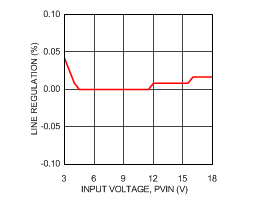
| ΔVOUT/ΔVIN | Line regulation | VPVIN = 3 V to 18 V | 0.01 | %/V | ||
| RDSonHS | High-side switch on-resistance | IDS = 5 A | 44 | mΩ | ||
| RDSonLS | Low-side switch on-resistance | IDS = 5 A | 22 | mΩ | ||
| ICL-HS | High-side switch current limit | High-side MOSFET | 5.9 | 7 | 7.87 | A |
| ICL-LS | Low-side switch current limit | Low-side MOSFET(3) | 5.9 | 8 | 10.2 | A |
| INEG-CL-LS | Low-side switch negative current limit | Low-side MOSFET | –7 | –4.1 | –1.64 | A |
| ISD | Quiescent current, disabled | VAVIN = V PVIN = 5 V | 0.1 | 2 | µA | |
| VAVIN = V PVIN = 18 V | 1 | 4.1 | ||||
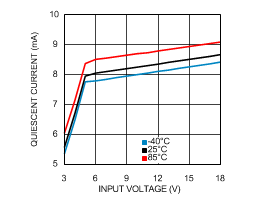
| IQ | Quiescent current, enabled, not switching | VAVIN = V PVIN = 18 V | 9 | 9.7 | mA | |
| IFB | Feedback pin input bias current | VFB = 0.598 V | 1 | nA | ||
| GM | Error amplifier transconductance | 2400 | µs | |||
| AVOL | Error amplifier voltage gain | 65 | dB | |||
| VIH-OVP | OVP tripping threshold | Rising threshold, percentage of VOUT | 103.5% | 109.5% | 115% | |
| VHYST-OVP | OVP hysteresis window | Percentage of VOUT | –4.3% | |||
| VUVLO-HI-AVIN | AVIN UVLO rising threshold | 2.84 | 2.93 | 2.987 | V | |
| VUVLO-LO-AVIN | AVIN UVLO falling threshold | 2.66 | 2.73 | 2.83 | V | |
| VUVLO-HYS-AVIN | AVIN UVLO hysteresis window | 195 | mV | |||
| V5V0 | Internal LDO1 output voltage | Measured at 5V0 pin, 1-kΩ load | 4.88 | V | ||
| COUT-CAP-5V0 | Recommended capacitance connected to 5V0 pin | Ceramic capacitor | 1 | µF | ||
| GENERAL (continued) | ||||||
| ISHORT-5V0 | Short-circuit current of 5V0 pin | 31 | mA | |||
| V2V5 | Internal LDO2 output voltage | Measured at 2V5 pin, 1-kΩ load | 2.47 | V | ||
| COUT-CAP-2V5 | Recommended capacitance connected to 2V5 pin | Ceramic capacitor | 100 | nF | ||
| ISHORT-2V5 | Short-circuit current of 2V5 pin | 47 | mA | |||
| VFCBOOT-D | CBOOT diode forward voltage | Measured from 5V0 to CBOOT at 10 mA | 0.76 | V | ||
| ICBOOT | CBOOT leakage current | VCBOOT = 5.5 V, not switching | 0.65 | µA | ||
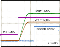
| TSTARTUP-DELAY | Startup time from EN high to the beginning of internal soft-start | 160 | µs | |||
| SS | Internal soft-start | 10% to 90% VFB | 1.41 | 2.7 | 4.15 | ms |
| OSCILLATOR | ||||||
| FOSC-NOM | Oscillator frequency, nominal measured at SW pin | RFRQ = 61.9 kΩ, 0.025% | 695 | 750 | 795 | kHz |
| FOSC-MAX | Maximum oscillator frequency measured at SW pin | RFRQ = 28.4 kΩ | 1500 | kHz | ||
| FOSC-MIN | Minimum oscillator frequency measured at SW pin | RFRQ = 167.5 kΩ | 300 | kHz | ||
| TOFF-MIN | Minimum off-time measured at SW pin | FSW = 1.5 MHz, VIN = 3.3 V, VFB = 1 V, voltage divider ratio = 3.3 | 50 | ns | ||
| TON-MIN | Minimum on-time measured at SW pin | FSW = 1.5 MHz, voltage divider ratio = 1 | 70 | ns | ||
| LOGIC | ||||||
| VIH-EN | EN pin rising threshold | 1.1 | 1.2 | 1.3 | V | |
| VHYST-EN | EN pin hysteresis window | 130 | 200 | 302 | mV | |
| IEN-IN | EN pin input current | VEN = 12 V | 18 | 23 | µA | |
| VIH-UV-PGOOD | PGOOD UV rising threshold | Percentage of VOUT | 87.5% | 93% | 97.5% | |
| VHYST-UV-PGOOD | PGOOD UV hysteresis threshold | Percentage of VOUT | –4.2% | |||
| IOL- PGOOD | PGOOD sink current | VOL = 0.2 V | 3 | mA | ||
| IOH- PGOOD | PGOOD leakage current | VOH = 18 V | 460 | nA | ||
| THERMAL SHUTDOWN | ||||||
| TSD | Thermal shutdown(4) | 160 | °C | |||
| TSD-HYS | Thermal shutdown hysteresis(4) | 10 | °C | |||
7.6 Typical Characteristics
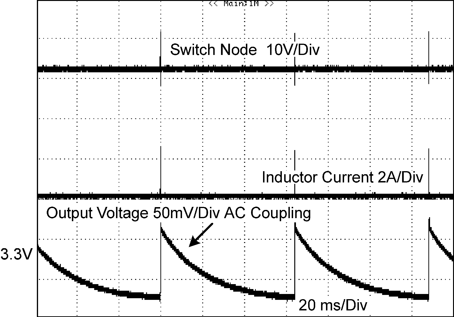
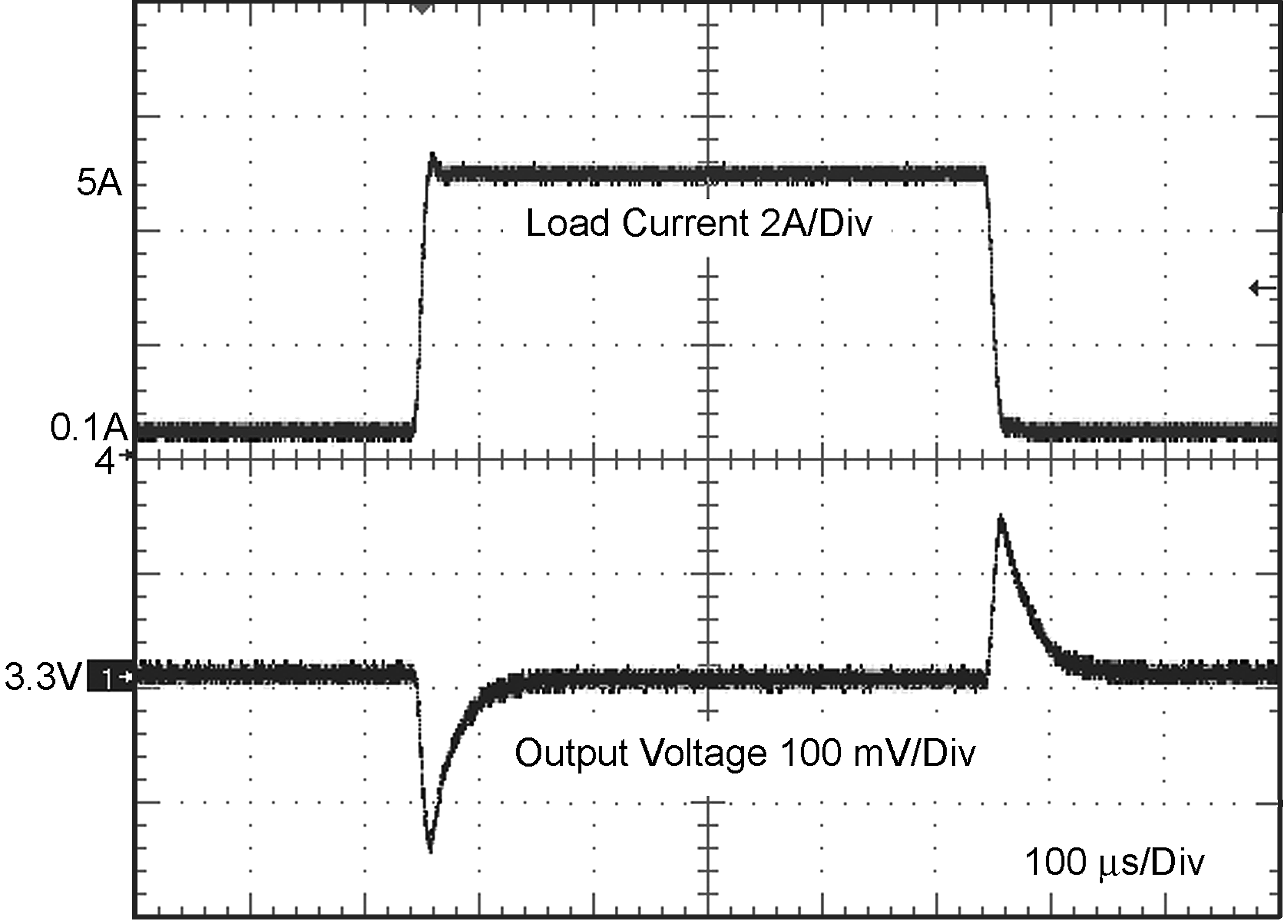
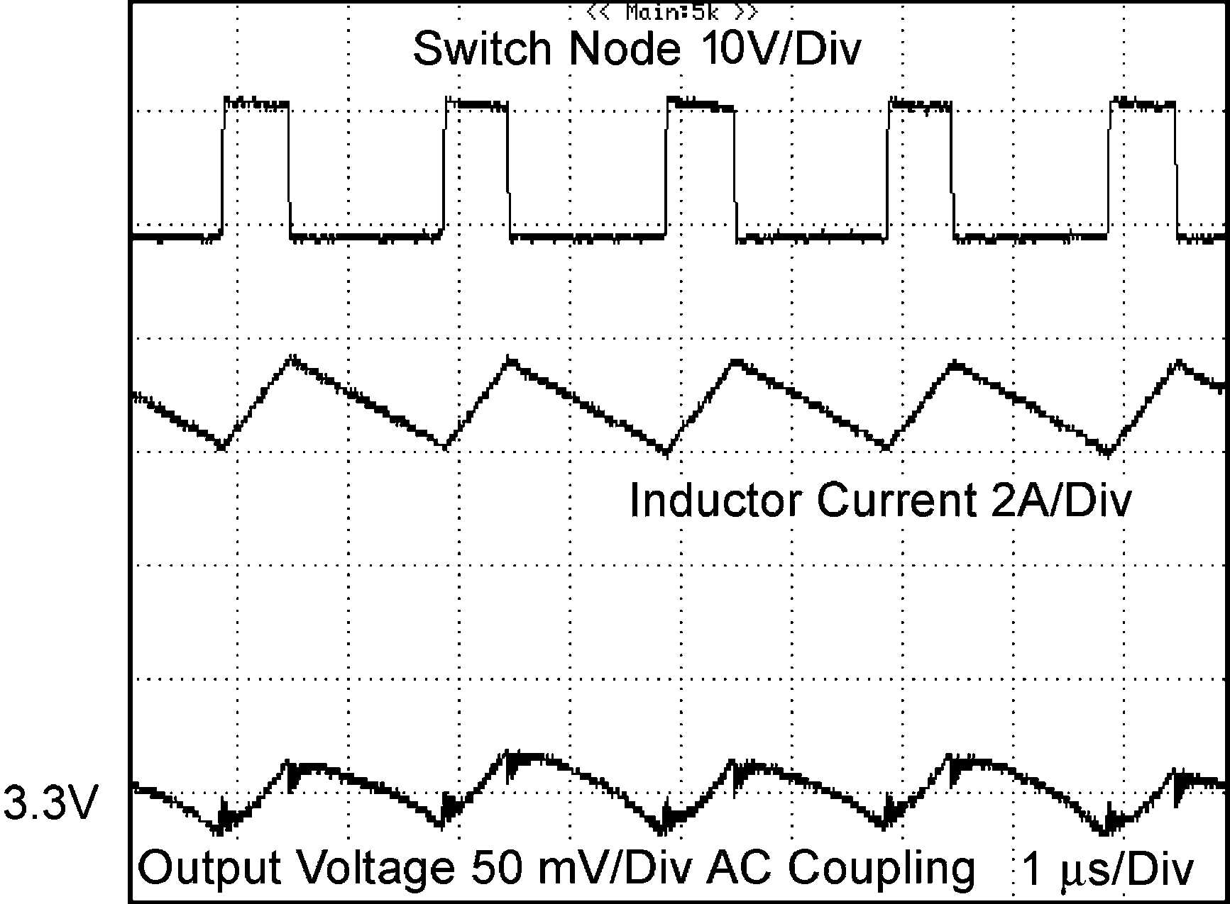
VIN = 12 V, VOUT = 3.3 V, FSW = 500 kHz, TA = 25°C, L = 3.3 µH, and COUT = 100 µF (ceramic), (unless otherwise specified)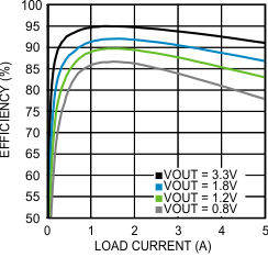
| FSW = 300 kHz |
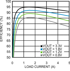
| FSW = 500 kHz |
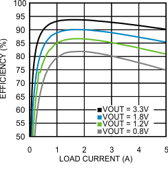
| FSW = 1 MHz |
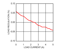
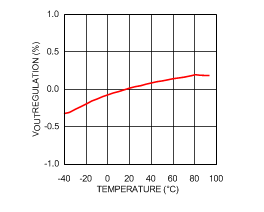
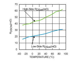
vs Temperature
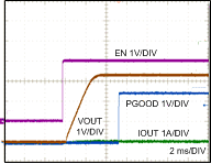
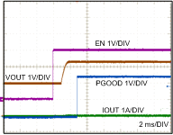
| FSW = 300 kHz |

| FSW = 500 kHz |
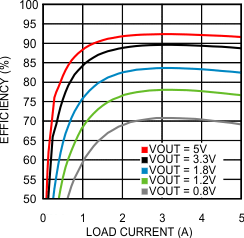
| FSW = 1 MHz |
