LM22672/-Q1 42-V, 1-A SIMPLE SWITCHER® Step-Down Voltage Regulator with Features
1 Features
- Wide Input Voltage Range: 4.5 V to 42 V
- Internally Compensated Voltage Mode Control
- Stable with Low ESR Ceramic Capacitors
- 200 mΩ N-Channel MOSFET
- Output Voltage Options:
-ADJ (Outputs as Low as 1.285 V)
-5.0 (Output Fixed to 5 V) - ±1.5% Feedback Reference Accuracy
- 500 kHz Default Switching Frequency
- Adjustable Switching Frequency and Synchronization
- –40°C to 125°C Junction Temperature Range
- Precision Enable Input
- Integrated Boot-Strap Diode
- Adjustable Soft-Start
- Fully WEBENCH® Enabled
- LM22672-Q1 is an Automotive Grade Product
that is AEC-Q100 Grade 1 Qualified (–40°C to +125°C Junction Temperature) - SO PowerPAD (Exposed Pad)
2 Applications
- Industrial Control
- Telecom and Datacom Systems
- Embedded Systems
- Conversions from Standard 24 V, 12 V and 5 V Input Rails
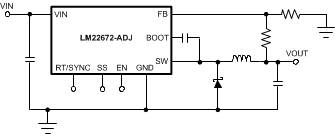
Simplified Application Schematic
3 Description
The LM22672 switching regulator provides all of the functions necessary to implement an efficient high voltage step-down (buck) regulator using a minimum of external components. This easy to use regulator incorporates a 42 V N-channel MOSFET switch capable of providing up to 1 A of load current. Excellent line and load regulation along with high efficiency (> 90%) are featured. Voltage mode control offers short minimum on-time, allowing the widest ratio between input and output voltages. Internal loop compensation means that the user is free from the tedious task of calculating the loop compensation components. Fixed 5 V output and adjustable output voltage options are available.
The default switching frequency is set at 500 kHz allowing for small external components and good transient response. In addition, the frequency can be adjusted over a range of 200 kHz to 1 MHz with a single external resistor. The internal oscillator can be synchronized to a system clock or to the oscillator of another regulator. A precision enable input allows simplification of regulator control and system power sequencing. In shutdown mode the regulator draws only 25 µA (typ). An adjustable soft-start feature is provided through the selection of a single external capacitor. The LM22672 also has built in thermal shutdown, and current limiting to protect against accidental overloads.
The LM22672 is a member of Texas Instruments' SIMPLE SWITCHER® family. The SIMPLE SWITCHER® concept provides for an easy to use complete design using a minimum number of external components and the TI WEBENCH® design tool. TI's WEBENCH® tool includes features such as external component calculation, electrical simulation, thermal simulation, and Build-It boards for easy design-in.
Device Information(1)
| PART NUMBER | PACKAGE | BODY SIZE (NOM) |
|---|---|---|
| LM22672, LM22672-Q1 |
HSOP (8) | 4.89 mm x 3.90 mm |
- For all available packages, see the orderable addendum at the end of the data sheet.
4 Revision History
Changes from L Revision (April 2013) to M Revision
- Added Pin Configuration and Functions section, Handling Rating table, Feature Description section, Device Functional Modes, Application and Implementation section, Power Supply Recommendations section, Layout section, Device and Documentation Support section, and Mechanical, Packaging, and Orderable Information section Go
Changes from K Revision (April 2013) to L Revision
- Changed from National to TI format Go
5 Pin Configuration and Functions

Pin Functions
| PIN | TYPE | DESCRIPTION | APPLICATION INFORMATION | |
|---|---|---|---|---|
| NAME | NO. | |||
| BOOT | 1 | I | Bootstrap input | Provides the gate voltage for the high side NFET. |
| EN | 5 | I | Enable input | Used to control regulator start-up and shutdown. See Precision Enable and UVLO section of data sheet. |
| EP | EP | — | Exposed Pad | Connect to ground. Provides thermal connection to PCB. See Thermal Considerations. |
| FB | 4 | I | Feedback input | Feedback input to regulator. |
| GND | 6 | — | Ground input to regulator; system common |
System ground pin. |
| RT/SYNC | Oscillator mode control input | Used to control oscillator mode of regulator. See Switching Frequency Adjustment and Synchronization section of data sheet. | ||
| SS | 2 | I | Soft-start input | Used to increase soft-start time. See Soft-Start section of data sheet. |
| SW | 8 | O | Switch output | Switching output of regulator. |
| VIN | I | Input voltage | Supply input to the regulator. | |
6 Specifications
6.1 Absolute Maximum Ratings(1)(2)
over operating free-air temperature range (unless otherwise noted)| MIN | MAX | UNIT | ||
|---|---|---|---|---|
| VIN to GND | 43 | V | ||
| EN Pin Voltage | –0.5 | 6 | V | |
| SS, RT/SYNC Pin Voltage | –0.5 | 7 | V | |
| SW to GND(3) | –5 | VIN | V | |
| BOOT Pin Voltage | VSW + 7 | V | ||
| FB Pin Voltage | –0.5 | 7 | V | |
| Power Dissipation | Internally Limited | |||
| Junction Temperature | 150 | °C | ||
| For soldering specifications, refer to Application Report Absolute Maximum Ratings for Soldering (SNOA549). | ||||
6.2 Handling Ratings: LM22672
| MIN | MAX | UNIT | |||
|---|---|---|---|---|---|
| Tstg | Storage temperature range | –65 | 150 | °C | |
| V(ESD) | Electrostatic discharge | Human body model (HBM), per ANSI/ESDA/JEDEC JS-001, all pins(1) | –2 | 2 | kV |
6.3 Handling Ratings: LM22672-Q1
| MIN | MAX | UNIT | ||||
|---|---|---|---|---|---|---|
| Tstg | Storage temperature range | –65 | 150 | °C | ||
| V(ESD) | Electrostatic discharge | Human body model (HBM), per AEC Q100-002(1) | –2 | 2 | kV | |
6.4 Recommended Operating Conditions
| MIN | MAX | UNIT | ||
|---|---|---|---|---|
| VIN | Supply Voltage | 4.5 | 42 | V |
| Junction Temperature Range | –40 | 125 | °C | |
6.5 Thermal Information
| THERMAL METRIC(1) | LM22672, LM22672-Q1 | UNIT | |||
|---|---|---|---|---|---|
| HSOP | |||||
| 8 PINS | |||||
| RθJA | Junction-to-ambient thermal resistance | MR Package, Junction to ambient thermal resistance(2) | 60 | °C/W | |
6.6 Electrical Characteristics
Typical values represent the most likely parametric norm at TA = TJ = 25°C, and are provided for reference purposes only. Unless otherwise specified: VIN = 12 V.| PARAMETER | TEST CONDITIONS | MIN(5) | TYP(4) | MAX(5) | UNIT | |
|---|---|---|---|---|---|---|
| LM22672-5.0 | ||||||
| VFB | Feedback Voltage | VIN = 8 V to 42 V | 4.925 | 5.0 | 5.075 | V |
| VIN = 8 V to 42 V, –40°C ≤ TJ ≤ 125°C | 4.9 | 5.1 | ||||
| LM22672-ADJ | ||||||
| VFB | Feedback Voltage | VIN = 4.7 V to 42 V | 1.266 | 1.285 | 1.304 | V |
| VIN = 4.7 V to 42 V, –40°C ≤ TJ ≤ 125°C | 1.259 | 1.311 | ||||
| ALL OUTPUT VOLTAGE VERSIONS | ||||||
| IQ | Quiescent Current | VFB = 5 V | 3.4 | mA | ||
| VFB = 5 V, –40°C ≤ TJ ≤ 125°C | 6 | |||||
| ISTDBY | Standby Quiescent Current | EN Pin = 0 V | 25 | 40 | µA | |
| ICL | Current Limit | 1.3 | 1.5 | 1.7 | A | |
| –40°C ≤ TJ ≤ 125°C | 1.2 | 1.8 | ||||
| IL | Output Leakage Current | VIN = 42 V, EN Pin = 0 V, VSW = 0 V | 0.2 | 2 | µA | |
| VSW = –1 V | 0.1 | 3 | µA | |||
| RDS(ON) | Switch On-Resistance | 0.2 | 0.24 | Ω | ||
| –40°C ≤ TJ ≤ 125°C | 0.32 | |||||
| Fsw | Oscillator Frequency | 500 | kHz | |||
| –40°C ≤ TJ ≤ 125°C | 400 | 600 | ||||
| TOFF | Minimum Off-time | 200 | ns | |||
| –40°C ≤ TJ ≤ 125°C | 100 | 300 | ||||
| TON | Minimum On-time | 100 | ns | |||
| IBIAS | Feedback Bias Current | VFB = 1.3 V (ADJ Version Only) | 230 | nA | ||
| VEN | Enable Threshold Voltage | Falling | 1.6 | V | ||
| Falling, –40°C ≤ TJ ≤ 125°C | 1.3 | 1.9 | ||||
| VENHYST | Enable Voltage Hysteresis | 0.6 | V | |||
| IEN | Enable Input Current | EN Input = 0 V | 6 | µA | ||
| FSYNC | Maximum Synchronization Frequency | VSYNC = 3.5 V, 50% duty-cycle | 1 | MHz | ||
| VSYNC | Synchronization Threshold Voltage | 1.75 | V | |||
| ISS | Soft-Start Current | 50 | µA | |||
| –40°C ≤ TJ ≤ 125°C | 30 | 70 | ||||
| TSD | Thermal Shutdown Threshold | 150 | °C | |||
6.7 Typical Characteristics
Vin = 12 V, TJ = 25°C (unless otherwise specified) Figure 1. Efficiency vs IOUT and VIN, VOUT = 3.3 V
 Figure 3. Current Limit vs Temperature
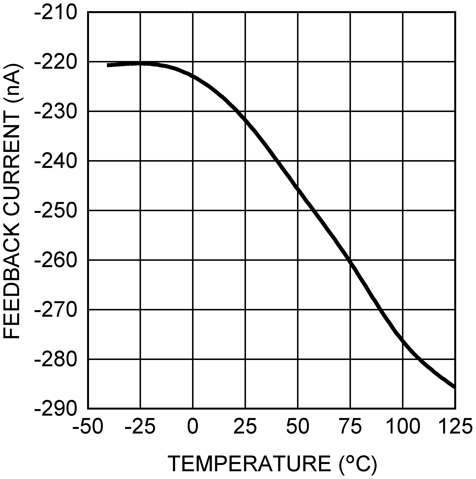 Figure 5. Feedback Bias Current vs Temperature
 Figure 7. Standby Quiescent Current vs Input Voltage
 Figure 9. Normalized Feedback Voltage vs Input Voltage
 Figure 11. Soft-Start Current vs Temperature
 Figure 2. Normalized Switching Frequency vs Temperature
 Figure 4. Normalized RDS(ON) vs Temperature
 Figure 6. Normalized Enable Threshold Voltage vs Temperature
 Figure 8. Normalized Feedback Voltage vs Temperature
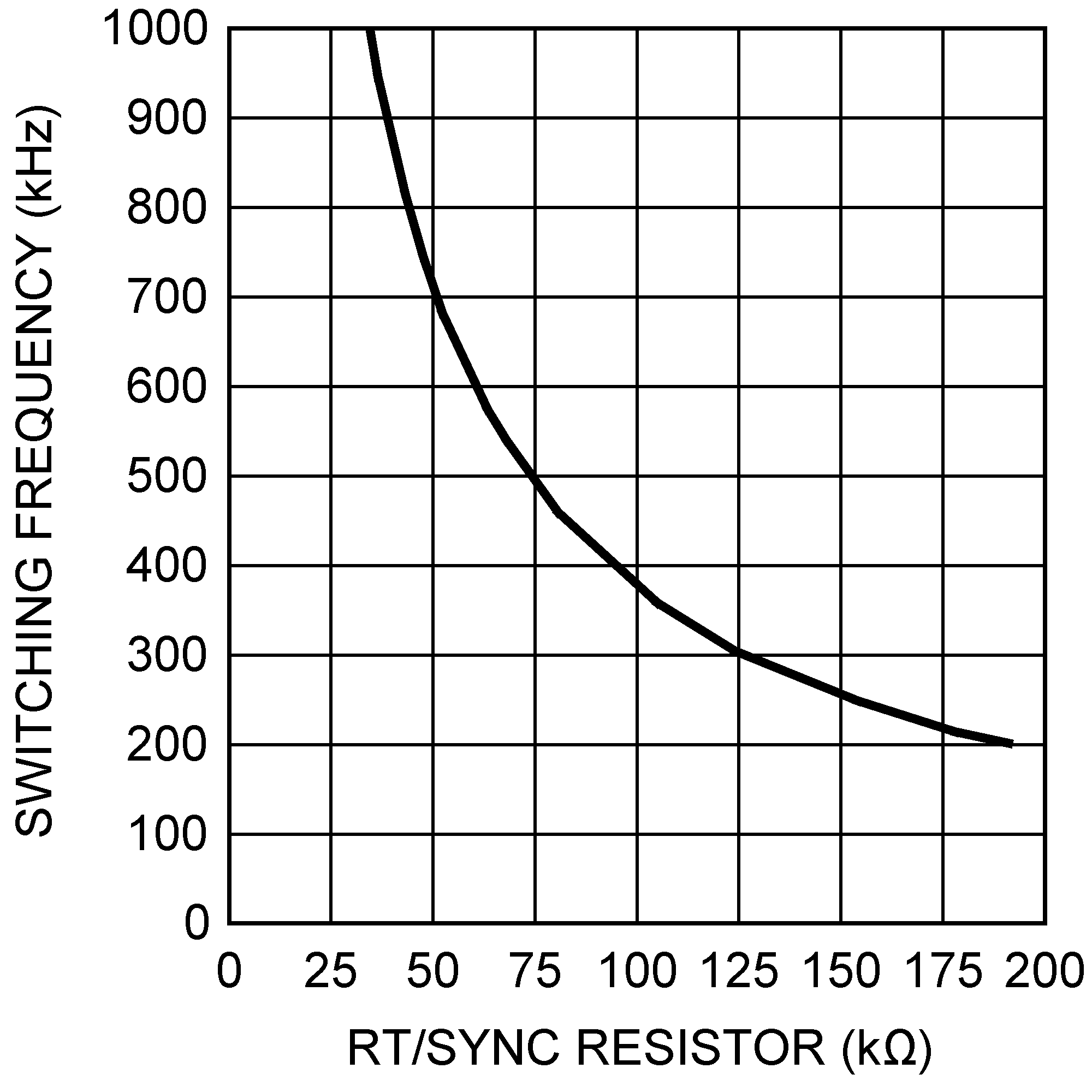 Figure 10. Switching Frequency vs RT/SYNC Resistor