-
LM26001/-Q1 1.5-A Switching Regulator With High-Efficiency Sleep Mode
- 1 Features
- 2 Applications
- 3 Description
- 4 Revision History
- 5 Pin Configuration and Functions
- 6 Specifications
- 7 Detailed Description
- 8 Applications and Implementation
- 9 Power Supply Recommendations
- 10Layout
- 11Device and Documentation Support
- 12Mechanical, Packaging, and Orderable Information
- IMPORTANT NOTICE
Package Options
Mechanical Data (Package|Pins)
- PWP|16
Thermal pad, mechanical data (Package|Pins)
- PWP|16
Orderable Information
LM26001/-Q1 1.5-A Switching Regulator With High-Efficiency Sleep Mode
1 Features
- LM26001-Q1 is an Automotive-Grade Product that is AEC-Q100 Grade 1 Qualified (–40°C to +125°C Operating Junction Temperature)
- High-Efficiency Sleep Mode
- 40-µA Typical Iq in Sleep Mode
- 10-µA Typical Iq in Shutdown Mode
- 3.0-V Minimum Input Voltage
- 4.0-V to 38-V Continuous Input Range
- 1.5% Reference Accuracy
- Cycle-by-Cycle Current Limit
- Adjustable Frequency (150 kHz to 500 kHz)
- Synchronizable to an External Clock
- Power Good Flag
- Forced PWM Function
- Adjustable Soft-Start
- HTSSOP-16 Exposed Pad Package
- Thermal Shut Down
2 Applications
- Automotive Telematics
- Navigation Systems
- In-Dash Instrumentation
- Battery-Powered Applications
- Standby Power for Home Gateways/Set-top Boxes
3 Description
The LM26001 is a switching regulator designed for the high-efficiency requirements of applications with standby modes. The device features a low-current sleep mode to maintain efficiency under light-load conditions and current-mode control for accurate regulation over a wide input voltage range. Quiescent current is reduced to 10 µA typically in shutdown mode and less than 40 µA in sleep mode. Forced PWM mode is also available to disable sleep mode.
The LM26001 can deliver up to 1.5 A of continuous load current with a fixed current limit, through the internal N-channel switch. The part has a wide input voltage range of 4.0 V to 38 V and can operate with input voltages as low as 3 V during line transients.
Operating frequency is adjustable from 150 kHz to 500 kHz with a single resistor and can be synchronized to an external clock.
Other features include Power Good, adjustable soft-start, enable pin, input undervoltage protection, and an internal bootstrap diode for reduced component count.
Device Information(1)
| PART NUMBER | PACKAGE | BODY SIZE (NOM) |
|---|---|---|
| LM26001 | HTSSOP (16) | 5.00 mm x 4.40 mm |
| LM26001-Q1 |
- For all available packages, see the orderable addendum at the end of the datasheet.
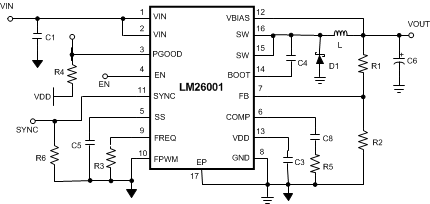
Typical Application Circuit

4 Revision History
Changes from H Revision (November 2014) to I Revision
- Update made to the Power Dissipation description in Section 6.1 Go
- Changed ESD Ratings to ± and moved storage temp to Absolute Maximum RatingsGo
Changes from G Revision (April 2013) to H Revision
- Added Pin Configuration and Functions section, Handling Rating table, Feature Description section, Device Functional Modes, Application and Implementation section, Power Supply Recommendations section, Layout section, Device and Documentation Support section, and Mechanical, Packaging, and Orderable Information section Go
Changes from F Revision (April 2013) to G Revision
- Changed layout of National Data Sheet to TI formatGo
5 Pin Configuration and Functions

Pin Functions
| PIN | I/O | DESCRIPTION | |
|---|---|---|---|
| NO. | NAME | ||
| 1 | VIN | A | Power supply input |
| 2 | VIN | A | Power supply input |
| 3 | PGOOD | O | Power Good pin. An open-drain output which goes high when the output voltage is greater than 92% of nominal. |
| 4 | EN | I | Enable is an analog level input pin. When pulled below 0.8 V, the device enters shutdown mode. |
| 5 | SS | A | Soft-start pin. Connect a capacitor from this pin to GND to set the soft-start time. |
| 6 | COMP | A | Compensation pin. Connect to a resistor capacitor pair to compensate the control loop. |
| 7 | FB | A | Feedback pin. Connect to a resistor divider between Vout and GND to set output voltage. |
| 8 | GND | G | Ground |
| 9 | FREQ | A | Frequency adjust pin. Connect a resistor from this pin to GND to set the operating frequency. |
| 10 | FPWM | I | FPWM is a logic level input pin. For normal operation, connect to GND. When pulled high, sleep mode operation is disabled. |
| 11 | SYNC | I | Frequency synchronization pin. Connect to an external clock signal for synchronized operation. SYNC must be pulled low for non-synchronized operation. |
| 12 | VBIAS | A | Connect to an external 3-V or greater supply to bypass the internal regulator for improved efficiency. If not used, VBIAS should be tied to GND. |
| 13 | VDD | A | The output of the internal regulator. Bypass with a minimum 1.0-µF capacitor. |
| 14 | BOOT | A | Bootstrap capacitor pin. Connect a 0.1-µF minimum ceramic capacitor from this pin to SW to generate the gate drive bootstrap voltage. |
| 15 | SW | A | Switch pin. The source of the internal N-channel switch. |
| 16 | SW | A | Switch pin. The source of the internal N-channel switch. |
| EP | EP | G | Exposed Pad thermal connection. Connect to GND. |