LM2941x 1-A Low Dropout Adjustable Regulator
1 Features
- Operating VIN Range: 6 V to 26 V
- Output Voltage Adjustable From 5 V to 20 V
- Dropout Voltage Typically 0.5 V at IOUT = 1 A
- Output Current in Excess of 1 A
- Trimmed Reference Voltage
- Reverse Battery Protection
- Internal Short-Circuit Current Limit
- Mirror Image Insertion Protection
- P+ Product Enhancement Tested
- TTL, CMOS Compatible ON/OFF Switch
- WSON Space-Saving Package
2 Applications
- Industrial
- Automotive
3 Description
The LM2941 positive voltage regulator features the ability to source 1 A of output current with a typical dropout voltage of 0.5 V and a maximum of 1 V over the entire temperature range. Furthermore, a quiescent current reduction circuit has been included which reduces the ground pin current when the differential between the input voltage and the output voltage exceeds approximately 3 V. The quiescent current with 1 A of output current and an input-output differential of 5 V is therefore only 30 mA. Higher quiescent currents only exist when the regulator is in the dropout mode (VIN − VOUT ≤ 3 V).
Designed also for vehicular applications, the LM2941 and all regulated circuitry are protected from reverse battery installations or two-battery jumps. During line transients, such as load dump when the input voltage can momentarily exceed the specified maximum operating voltage, the regulator will automatically shut down to protect both the internal circuits and the load. Familiar regulator features such as short circuit and thermal overload protection are also provided.
Device Information(1)
| PART NUMBER | PACKAGE | BODY SIZE (NOM) |
|---|---|---|
| LM2941 | WSON (8) | 4.00 mm x 4.00 mm |
| TO-263 (5) | 10.16 mm x 8.42 mm | |
| TO-220 (5) | 14.986 mm x 10.16 mm | |
| TO-220 (5) | 10.16 mm x 8.51 mm | |
| LM2941C | TO-263 (5) | 10.16 mm x 8.42 mm |
| TO-220 (5) | 14.986 mm x 10.16 mm | |
| TO-220 (5) | 10.16 mm x 8.51 mm |
- For all available packages, see the orderable addendum at the end of the datasheet.

4 Revision History
Changes from H Revision (December 2014) to I Revision
- Changed update pin names to TI nomenclature Go
Changes from G Revision (April 2013) to H Revision
- Added Device Information and ESD Ratings tables, Feature Description section, Device Functional Modes, Application and Implementation section, Power Supply Recommendations section, Layout section, Device and Documentation Support section, and Mechanical, Packaging, and Orderable Information section; updated Thermal InfoGo
Changes from F Revision (April 2013) to G Revision
- Changed layout of National Data Sheet to TI formatGo
5 Pin Configuration and Functions


Pin Functions
| PIN | TYPE | DESCRIPTION | |||
|---|---|---|---|---|---|
| NAME | KC | KTT | NGN | ||
| ADJ | 1 | 1 | 8 | I | Sets output voltage |
| ON/OFF | 2 | 2 | 1 | I | Enable/Disable control |
| GND | 3 | 3 | 2, 7 | — | Ground |
| IN | 4 | 4 | 3 | I | Input supply |
| OUT | 5 | 5 | 5 | O | Regulated output voltage. This pin requires an output capacitor to maintain stability. See the Detailed Design Procedure section for output capacitor details. |
| NC | — | — | 4, 6 | — | No internal connection. Connect to GND or leave open. |
6 Specifications
6.1 Absolute Maximum Ratings(1)(2)
| MIN | MAX | UNIT | ||
|---|---|---|---|---|
| Input voltage (Survival Voltage, ≤ 100 ms) | LM2941T, LM2941S, LM2941LD | 60 | V | |
| LM2941CT, LM2941CS | 45 | V | ||
| Internal power dissipation (3) | Internally Limited | |||
| Maximum junction temperature | 150 | °C | ||
| Soldering remperature(4) | TO-220 (T), Wave, 10 s | 260 | °C | |
| TO-263 (S), 30 s | 235 | °C | ||
| WSON-8 (LD), 30 s | 235 | °C | ||
| Storage temperature, Tstg | −65 | 150 | °C | |
6.2 ESD Ratings
| VALUE | UNIT | |||
|---|---|---|---|---|
| V(ESD) | Electrostatic discharge | Human-body model (HBM), per ANSI/ESDA/JEDEC JS-001(1) | ±2000 | V |
6.3 Recommended Operating Conditions
| MIN | MAX | UNIT | ||
|---|---|---|---|---|
| Temperatures | LM2941T | −40 | 125 | °C |
| LM2941CT | 0 | 125 | ||
| LM2941S | −40 | 125 | ||
| LM2941CS | 0 | 125 | ||
| LM2941LD | −40 | 125 | ||
6.4 Thermal Information
| THERMAL METRIC(1)(3) | LM2941LD | LM2941S, LM2941T | UNIT | ||
|---|---|---|---|---|---|
| WSON (NGN) | TO-263 (KTT) | TO-220 (KC) | |||
| 8 PINS | 5 PINS | 5 PINS | |||
| RθJA | Junction-to-ambient thermal resistance | 40.5 | 41 | 32.1 | °C/W |
| RθJC(top) | Junction-to-case (top) thermal resistance | 26.2 | 43.2 | 25.6 | |
| RθJB | Junction-to-board thermal resistance | 17 | 22.9 | 18.3 | |
| ψJT | Junction-to-top characterization parameter | 0.2 | 11.4 | 8.5 | |
| ψJB | Junction-to-board characterization parameter | 17.2 | 21.9 | 17.7 | |
| RθJC(bot) | Junction-to-case (bottom) thermal resistance | 3.2 | 0.9 | 0.7 | |
6.5 Electrical Characteristics: LM2941T, LM2941S, LM2941LD
5 V ≤ VOUT ≤ 20 V, VIN = VOUT + 5 V, COUT = 22 μF, unless otherwise specified. MIN (minimum) and MAX (maximum) specifications in apply over the full Operating Temperature Range (unless otherwise specified) and typical values apply at TJ = 25°C.| PARAMETER | TEST CONDITIONS | MIN | TYP | MAX | UNIT |
|---|---|---|---|---|---|
| Reference voltage | 5 mA ≤ IOUT ≤ 1 A(1) | 1.211 | 1.275 | 1.339 | V |
| 5 mA ≤ IOUT ≤ 1 A(1), TJ = 25°C | 1.237 | 1.275 | 1.313 | ||
| Line regulation | VOUT + 2 V ≤ VIN ≤ 26 V, IOUT = 5 mA | 4 | 10 | mV/V | |
| Load regulation | 50 mA ≤ IOUT ≤ 1 A | 7 | 10 | mV/V | |
| Output impedance | 100 mADC and 20 mArms, ƒOUT = 120 Hz | 7 | mΩ/V | ||
| Quiescent current | VOUT + 2 V ≤ VIN < 26 V, IOUT = 5 mA | 10 | 20 | mA | |
| VOUT + 2 V ≤ VIN < 26 V, IOUT = 5 mA, TJ = 25°C | 10 | 15 | |||
| VIN = VOUT + 5 V, IOUT = 1 A | 30 | 60 | mA | ||
| VIN = VOUT + 5 V, IOUT = 1 A, TJ = 25°C | 30 | 45 | |||
| RMS output noise, % of VOUT | 10 Hz to 100 kHz, IOUT = 5 mA | 0.003% | |||
| Ripple rejection | ƒOUT = 120 Hz, 1 Vrms, IL = 100 mA | 0.005 | 0.04 | %/V | |
| ƒOUT = 120 Hz, 1 Vrms, IL = 100 mA, TJ = 25°C | 0.005 | 0.02 | |||
| Long-term stability | 0.4 | %/1000 Hr | |||
| Dropout voltage | IOUT = 1 A | 0.5 | 1 | V | |
| IOUT = 1 A, TJ = 25°C | 0.5 | 0.8 | |||
| IOUT = 100 mA | 110 | 200 | mV | ||
| Short-circuit current | VIN max = 26 V(2) | 1.6 | 1.9 | A | |
| Maximum line transient | VOUT max 1 V above nominal VOUT
ROUT = 100 Ω, t ≤ 100 ms |
60 | 75 | V | |
| Maximum operational input voltage | 26 | 31 | VDC | ||
| Reverse polarity DC input voltage |
ROUT = 100 Ω, VOUT ≥ −0.6 V | −15 | −30 | V | |
| Reverse polarity transient input voltage |
t ≤ 100 ms, ROUT = 100 Ω | −50 | −75 | ||
| ON/OFF threshold voltage ON |
IOUT ≤ 1 A | 1.30 | 0.80 | V | |
| ON/OFF threshold voltage OFF |
IOUT ≤ 1 A | 2 | 1.3 | ||
| ON/OFF threshold current |
VON/OFF = 2 V, IOUT ≤ 1 A | 50 | 300 | μA | |
| VON/OFF = 2 V, IOUT ≤ 1 A, TJ = 25°C | 50 | 100 |
6.6 Electrical Characteristics: LM2941CT, LM2941CS
5 V ≤ VOUT ≤ 20 V, VIN = VOUT + 5 V, COUT = 22 μF, unless otherwise specified. MIN (minimum) and MAX (maximum) specifications in apply over the full Operating Temperature Range (unless otherwise specified) and typical values apply at TJ = 25°C.| PARAMETER | TEST CONDITIONS | MIN | TYP | MAX | UNIT |
|---|---|---|---|---|---|
| Reference voltage | 5 mA ≤ IOUT ≤ 1 A(1) | 1.211 | 1.275 | 1.339 | V |
| 5 mA ≤ IOUT ≤ 1 A(1), TJ = 25°C | 1.237 | 1.275 | 1.313 | ||
| Line regulation | VOUT + 2 V ≤ VIN ≤ 26 V, IOUT = 5 mA, TJ = 25°C | 4 | 10 | mV/V | |
| Load regulation | 50 mA ≤ IOUT ≤ 1 A, TJ = 25°C | 7 | 10 | mV/V | |
| Output impedance | 100 mADC and 20 mArms, ƒOUT = 120 Hz | 7 | mΩ/V | ||
| Quiescent current | VOUT + 2 V ≤ VIN < 26 V, IOUT = 5 mA, TJ = 25°C | 10 | 15 | mA | |
| VIN = VOUT + 5 V, IOUT = 1 A | 30 | 60 | mA | ||
| VIN = VOUT + 5 V, IOUT = 1 A, TJ = 25°C | 30 | 45 | |||
| RMS output noise, % of VOUT | 10 Hz to 100 kHz IOUT = 5 mA |
0.003% | |||
| Ripple rejection | ƒOUT = 120Hz, 1 Vrms, IL = 100 mA, TJ = 25°C | 0.005 | 0.02 | %/V | |
| Long-term stability | 0.4 | %/1000 Hr | |||
| Dropout voltage | IOUT = 1A | 0.5 | 1 | V | |
| IOUT = 1A, TJ = 25°C | 0.5 | 0.8 | |||
| IOUT = 100 mA | 110 | 200 | mV | ||
| Short-circuit current | VIN max = 26 V(2), TJ = 25°C | 1.6 | 1.9 | A | |
| Maximum line transient | VOUT max 1 V above nominal VOUT, ROUT = 100 Ω, t ≤ 100 ms, , TJ = 25°C | 45 | 55 | V | |
| Maximum operational input voltage | TJ = 25°C | 26 | 31 | VDC | |
| Reverse polarity DC input voltage |
ROUT = 100 Ω, VOUT ≥ −0.6 V, TJ = 25°C | −15 | −30 | V | |
| Reverse polarity transient input voltage |
t ≤ 100 ms, ROUT = 100 Ω, TJ = 25°C | −45 | −55 | ||
| ON/OFF threshold voltage ON |
IOUT ≤ 1 A, TJ = 25°C | 1.3 | 0.8 | V | |
| ON/OFF threshold voltage OFF |
IOUT ≤ 1 A, TJ = 25°C | 2 | 1.3 | ||
| ON/OFF threshold current |
VON/OFF = 2 V, IOUT ≤ 1 A, TJ = 25°C | 50 | 100 | μA |
6.7 Typical Characteristics


7 Detailed Description
7.1 Overview
The LM2941 positive voltage regulator features the ability to source 1 A of output current with a dropout voltage of typically 0.5 V and a maximum of 1 V over the entire temperature range. Furthermore, a quiescent current reduction circuit has been included which reduces the ground current when the differential between the input voltage and the output voltage exceeds approximately 3 V. The quiescent current with 1 A of output current and an input-output differential of 5 V is therefore only 30 mA. Higher quiescent currents only exist when the regulator is in the dropout mode (VIN – VOUT ≤ 3 V).
7.2 Functional Block Diagram

7.3 Feature Description
7.3.1 Short-Circuit Current Limit
The internal current limit circuit is used to protect the LDO against high-load current faults or shorting events. The LDO is not designed to operate in a steady-state current limit. During a current-limit event, the LDO sources constant current. Therefore, the output voltage falls when load impedance decreases. Note also that if a current limit occurs and the resulting output voltage is low, excessive power may be dissipated across the LDO, resulting a thermal shutdown of the output.
7.3.2 Overvoltage Shutdown (OVSD)
Input voltage greater than typically 30 V will cause the LM2941 output to be disabled. When operating with the input voltage greater than the maximum recommended input voltage of 26 V, the device performance is not ensured. Continuous operation with the input voltage greater than the maximum recommended input voltage is discouraged.
7.3.3 Thermal Shutdown (TSD)
The LM2941 contains the thermal shutdown circuitry to turn off the output when excessive heat is dissipated in the LDO. The internal protection circuitry of the LM2941 is designed to protect against thermal overload conditions. The TSD circuitry is not intended to replace proper heat sinking. Continuously running the device into thermal shutdown degrades its reliability as the junction temperature will be exceeding the absolute maximum junction temperature rating.
7.3.4 Thermal Overload Protection
The LM2941 incorporates a linear form of thermal protection that limits the junction temperature (TJ) to typically 155°C.
Should the LM2941 see a fault condition that results in excessive power dissipation and the junction temperature approaches 155°C, the device will respond by reducing the output current (which reduces the power dissipation) to hold the junction temperature at 155°C.
Thermal Overload protection is not an ensured operating condition. Operating at, or near to, the thermal overload condition for any extended period of time is not encouraged, or recommended, as this may shorten the lifetime of the device.
7.4 Device Functional Modes
7.4.1 Operation With ON/OFF Control
The ON/OFF pin has no internal pull-up or pull-down to establish a default condition and, as a result, this pin must be terminated externally, either actively or passively. The ON/OFF pin requires a low level to enable the output, and a high level to disable the output. To ensure reliable operation, the ON/OFF pin voltage must rise above the maximum ON/OFF(OFF) voltage threshold (2 V) to disable the output, and must fall below the minimum ON/OFF(ON) voltage threshold (0.8 V) to enable the output. If the ON/OFF function is not needed this pin can be connected directly to Ground. If the ON/OFF pin is being pulled to a high state through a series resistor, an allowance must be made for the ON/OFF pin current that will cause a voltage drop across the pull-up resistor
8 Application and Implementation
NOTE
Information in the following applications sections is not part of the TI component specification, and TI does not warrant its accuracy or completeness. TI’s customers are responsible for determining suitability of components for their purposes. Customers should validate and test their design implementation to confirm system functionality.
8.1 Application Information
Figure 18 shows the typical application circuit for the LM2941. The output capacitor, COUT, must have a capacitance value of at least 22 µF with an equivalent series resistance (ESR) of at least 100 mΩ, but no more than 1 Ω. The minimum capacitance value and the ESR requirements apply across the entire expected operating ambient temperature range.
8.2 Typical Application

Note: Using 1 kΩ for R1 will ensure that the bias current error from the adjust pin will be negligible. Do not bypass R1 or R2. This will lead to instabilities.
* Required if regulator is located far from power supply filter.
** COUT must be at least 22 μF to maintain stability. May be increased without bound to maintain regulation during transients. Locate as close as possible to the regulator. This capacitor must be rated over the same operating temperature range as the regulator and the ESR is critical.
8.2.1 Design Requirements
| DESIGN PARAMETER | EXAMPLE VALUE |
|---|---|
| Input voltage range | 10 V to 26 V |
| Output voltage | 15 V |
| Output current range | 5 mA to 1 A |
| Input capacitor value | 0.47 µF |
| Output capacitor value | 22 µF minimum |
| Output capacitor ESR range | 100 mΩ to 1 Ω |
8.2.2 Detailed Design Procedure
8.2.2.1 Output Capacitor
A tantalum capacitor with a minimum capacitance value of 22 μF, and ESR in the range of 0.01 Ω to 5 Ω, is required at the output pin for loop stability. It must be located less than 1 cm from the device. There is no limitation on any additional capacitance.
Alternately, a high quality X5R/X7R 22 μF ceramic capacitor may be used for the output capacitor only if an appropriate value of series resistance is added to simulate the ESR requirement. The ceramic capacitor selection must include an appropriate voltage de-rating of the capacitance value due to the applied output voltage. The series resistor (for ESR simulation) should be in the range of 0.1 Ω to 1 Ω.
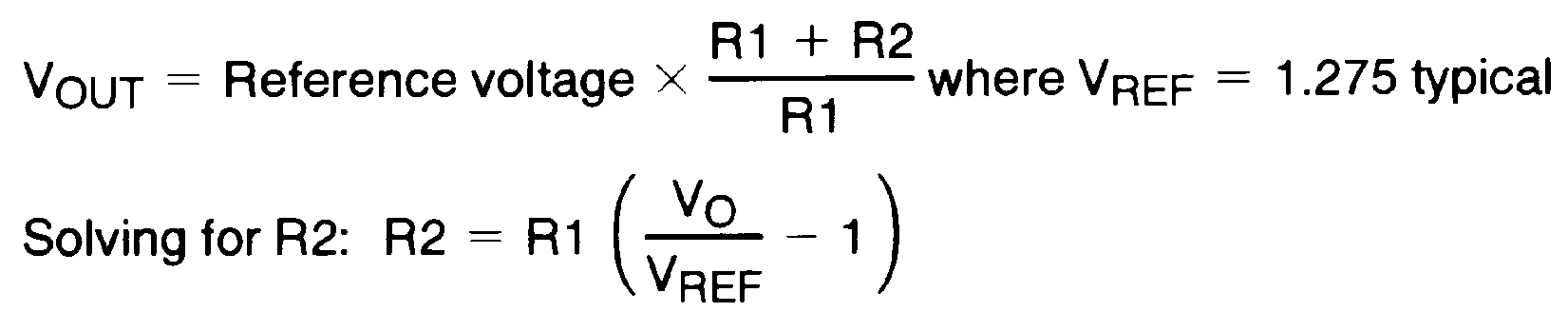
8.2.2.2 Setting the Output Voltage
The output voltage range is 5 V to 20 V and is set by the two external resistors, R1 and R2. See the Figure 18. The output voltage is given by the formula:
where
- VREF is typically 1.275 V
Using 1 kΩ for R1 will ensure that the bias current error of the adjust pin will be negligible. Using a R1 value higher than 10 kΩ may cause the output voltage to shift across temperature due to variations in the adjust pin bias current.
Calculating the upper resistor (R2) value of the pair when the lower resistor (R1) value is known is accomplished with the following formula:
The resistors used for R1 and R2 should be high quality, tight tolerance, and with matching temperature coefficients. It is important to remember that, although the value of VREF is ensured, the final value of VOUT is not. The use of low quality resistors for R1 and R2 can easily produce a VOUT value that is unacceptable.
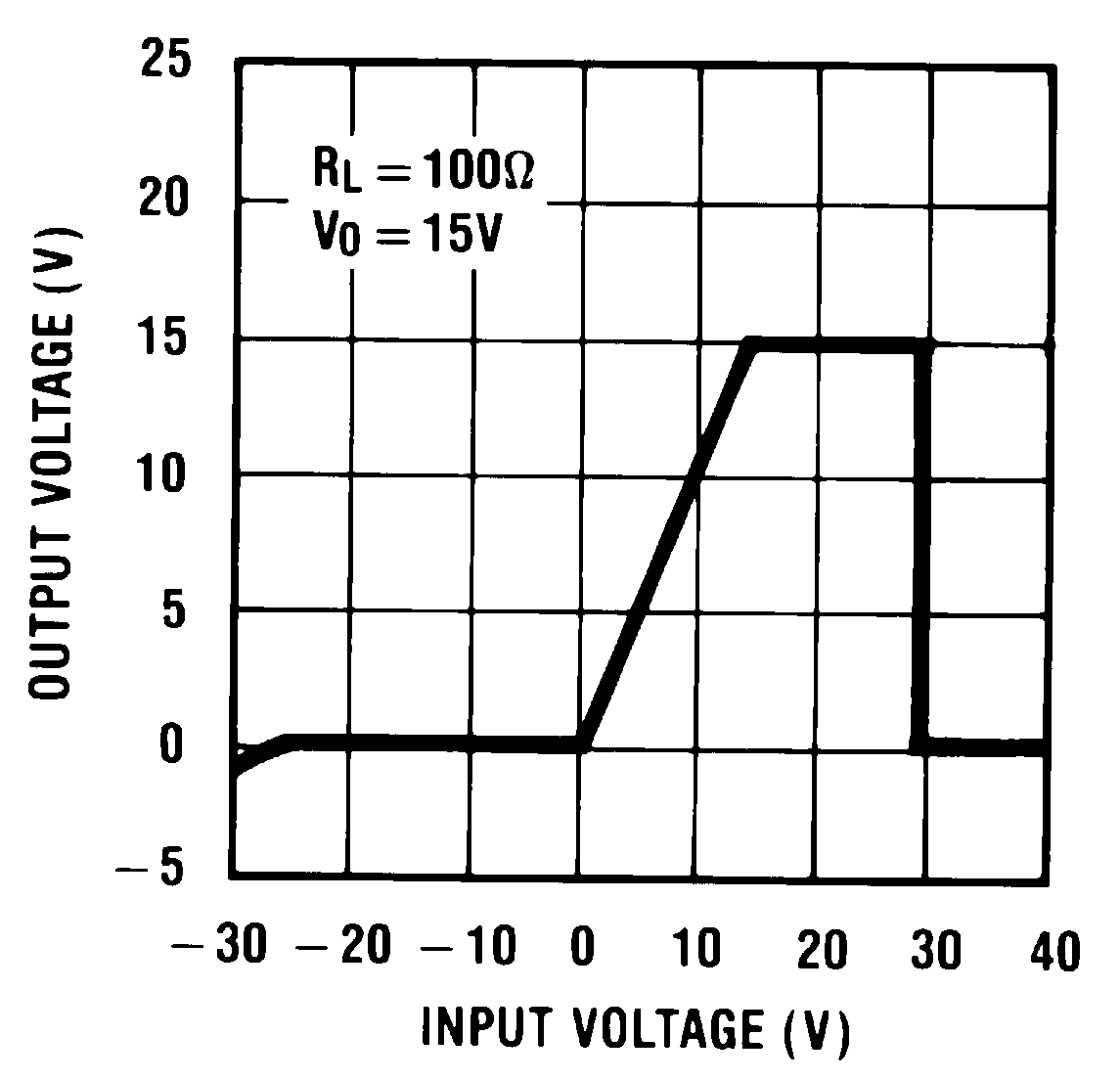
8.2.3 Application Curves
Figure 19. Low Voltage Behavior
Figure 20. Output at Voltage Extremes