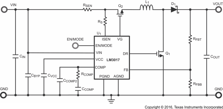
The LM3017 device is a versatile low-side NFET controller incorporating true shutdown and input side current limiting. The LM3017 is designed for simple implementation of boost conversions in Thunderbolt™ Technology. The LM3017 can also be configured for flyback or SEPIC designs. The input voltage range of 5 V to 18 V accommodates a two- or three-cell lithium ion battery or a 12-V rail. The enable pin accepts a single input to drive three different modes of operation: boost, pass-through, or shutdown mode. The LM3017 draws very low current in shutdown mode, typically 40 nA from the input supply.
The LM3017 provides an adjustable output to drive the Power Load Switch or MUX for the host Thunderbolt™ port. The ability to drive an external high-side NMOS provides for true isolation of the load from the input. Current limiting on the input ensures that inrush and short-circuit currents are always under control. The LM3017 incorporates built-in thermal shutdown, cycle-by-cycle current limit, short-circuit protection, output overvoltage protection, and soft start. It is available in a 10-pin WQFN package.
PART NUMBER | PACKAGE | BODY SIZE (NOM) |
---|---|---|
LM3017 | WQFN (10) | 2.40 mm × 2.70 mm |
Changes from C Revision (March 2013) to D Revision
Changes from B Revision (November 2012) to C Revision
PIN | TYPE(1) | DESCRIPTION | ||
---|---|---|---|---|
NO. | NAME | |||
1 | VCC | O | Driver supply voltage pin: output of internal regulator powering low side NMOS driver. A minimum of 0.47 µF must be connected from this pin to PGND for proper operation. | |
2 | DR | O | Low-side NMOS gate driver output: output gate drive to low side NMOS gate. | |
3 | PGND | G | Power ground: ground for power section. External power circuit reference. Must be connected to AGND at a single point. | |
4 | VG | O | High side NMOS gate driver output: output gate drive to high side NMOS gate. | |
5 | EN/MODE | A | Multi-function input pin: this input provides for chip enable, and mode selection. See Device Functional Modes for details. | |
6 | FB | A | Feed-back input pin: negative input to error amplifier. Connect to feedback resistor tap to regulate output. | |
7 | COMP | A | Compensation pin: a resistor and capacitor combination connected to this pin provides frequency compensation for the regulator control loop. | |
8 | AGND | G | Analog ground: ground for analog control circuitry. Reference point for all stated voltages. | |
9 | ISEN | A | Current sense input: current sense input, with respect to VIN, for all current limit functions. | |
10 | VIN | P | Power supply input pin: input supply to regulator. See Application and Implementation for recommendations on bypass capacitors on this pin. |
MIN | MAX | UNIT | ||
---|---|---|---|---|
VIN to PGND, AGND | –0.3 | 20 | V | |
FB, COMP, VCC,DR to PGND, AGND | –0.2 | 6 | V | |
EN/MODE | –0.2 | 5.5 | V | |
VG | –0.3 | VIN + 6 | V | |
ISEN to PGND, AGND | VIN – 0.3 | VIN | V | |
Peak low side driver output current | 1 | A | ||
Power dissipation | Internally limited | |||
Junction temperature, TJ | 150 | °C | ||
Storage temperature, Tstg | –65 | 150 | °C |
VALUE | UNIT | |||
---|---|---|---|---|
V(ESD) | Electrostatic discharge | Human-body model (HBM), per ANSI/ESDA/JEDEC JS-001(1) | ±1500 | V |
MIN | MAX | UNIT | ||
---|---|---|---|---|
VIN | Supply voltage | 5.4 | 18 | V |
TJ | Junction temperature | –40 | 125 | °C |
THERMAL METRIC(1) | LM3017 | UNIT | |
---|---|---|---|
NKL (WQFN) | |||
10 PINS | |||
RθJA | Junction-to-ambient thermal resistance | 79.2 | °C/W |
RθJC(top) | Junction-to-case (top) thermal resistance | 29.8 | °C/W |
RθJB | Junction-to-board thermal resistance | 21.4 | °C/W |
ψJT | Junction-to-top characterization parameter | 0.6 | °C/W |
ψJB | Junction-to-board characterization parameter | 20.7 | °C/W |
RθJC(bot) | Junction-to-case (bottom) thermal resistance | — | °C/W |
PARAMETER | TEST CONDITIONS | MIN(1) | TYP(2) | MAX(1) | UNIT | |
---|---|---|---|---|---|---|
VFB | Feedback voltage | Vcomp = 1.4 V | 1.256 | 1.27 | 1.282 | V |
ΔVLINE | Feedback voltage line regulation | 5 V ≤ VIN ≤ 18 V | 0.33% | |||
VUVLO | Input undervoltage lockout voltage | Rising | 4.6 | 4.82 | 4.9 | V |
Input undervoltage lockout hysteresis | Falling, below VUVLO | 280 | mV | |||
FSW | Nominal switching frequency | EN/MODE = 1.6 V | 550 | 600 | 635 | kHz |
RDS(ON) | Low-side NMOS driver resistance, top driver FET |
VIN = 5 V, IDR = 0.2 A | 3.4 | Ω | ||
Low-side NMOS driver resistance, bottom driver FET |
VIN = 5 V, IDR = 0.2 A | 1 | ||||
VCC | Driver voltage supply | VIN < 6 V | VIN | V | ||
VIN ≥ 6 V | 5.6 | |||||
Dmax | Maximum duty cycle | 86% | ||||
Tmin(on) | Minimum on-time | 125 | ns | |||
IQ-boost | Supply current in boost mode, no switching |
EN/MODE = 1.6 V, FB = 1.4 V | 5.2 | 9 | mA | |
IQ-SD | Supply current in shutdown mode | EN/MODE pin = 0.4 V | 0.025 | 1 | µA | |
IQ-pass | Supply current in pass-through mode | EN/MODE = 2.6 V, FB = 1.4 V | 1.4 | 2.3 | mA | |
Ven-pass | Pass-through mode threshold(3) | Rising | 2.19 | 2.4 | 2.56 | V |
Vmode-hyst | Mode change hysteresis, falling(3) | Falling | 65 | 107 | 165 | V |
Ven-shutdown | Shutdown mode threshold(3) | Falling | 0.2 | 0.4 | 0.59 | V |
Ven-boost | Boost mode enable window(3) | Rising | 0.65 | 1.22 | 1.6 | V |
Ien | EN/MODE pin bias current(4) | EN/MODE = 1.6 V | ±1 | µA | ||
VSENSE | Cycle-by-cycle current limit threshold during boost mode | EN/MODE = 1.6 V, FB = 50 V | 142 | 170 | 182 | mV |
ΔVSC | Short-circuit current limit threshold during boost mode | EN/MODE = 1.6 V, FB = 0 V | 18 | 30 | 42 | mV |
VSL | Internal ramp compensation voltage | 90 | mV | |||
VLIM1 | Input current limit threshold voltage in pass-through mode during TLIM1(3) | EN/MODE = 2.6 V | 70 | 85 | 95 | mV |
ΔVLIM2 | Input current limit threshold voltage in pass-through mode during TLIM2(3) | EN/MODE = 2.6 V | 14.5 | 18 | 21 | mV |
TLIM1 | Curent limit time at TLIM1(3) | 900 | µs | |||
TLIM2 | Current limit time at TLIM2(3) | 3.6 | ms | |||
TSC | Current limit time at TSC(3) | 900 | µs | |||
VOVP | Upper-output overvoltage protection threshold | Rising threshold measured at FB pin with respect to FB pin, VCOMP = 1.45 V | 40 | mV | ||
Lower-output overvoltage protection threshold | Falling threshold measured at FB pin with respect to FB pin, VCOMP = 1.45 V | 26 | ||||
VGS-on | On-state drive voltage at VG pin(5) | VIN = 5 V, ISEN = 5 V, IG = 0 A | 3.8 | 4.9 | V | |
VGS-off | Off-state drive voltage at VG pin(6) | Vin = 5 V, ISEN = VIN – 200 mV, IG = 0 A | 5 | mV | ||
IG | Maximum drive current at VG pin | VIN = 5 V, ISEN = 5 V, VG = VIN | 20 | µA | ||
Gm | Error amplifier transconductance | VCOM = 1.4 V, ICOMP = ±50 µA | 340 | 522 | 900 | µA/V |
AVOL | Error amplifier open-loop voltage gain | VCOM = 1.2 V to 1.8 V, ICOMP = 0 A | 190 | 313 | 450 | V/V |
RO | Error amplifier open-loop output resistance(7) | 600 | kΩ | |||
IEAO | Error amplifier output current swings | Sourcing: VCOMP = 1.4 V, VFB = 1.1 V | 27 | 66 | 115 | µA |
Sinking: VCOMP = 1.4 V, VFB = 1.4 V | 49 | 68 | 125 | |||
VEAO | Error amplifier output voltage limits | Upper: VFB = 0 V, COMP pin floating | 2.3 | V | ||
Lower: VFB = 1.4 V | 0.82 | |||||
Tr | Drive pin rise time | Cload = 3 nF, VDR = 0 V to 3 V | 25 | ns | ||
Tf | Drive pin fall time | Cload = 3 nF, VDR = 3 V to 0 V | 25 | ns | ||
TSD | Thermal shutdown threshold | 165 | °C | |||
TSD-hyst | Thermal shutdown threshold hysteresis | 10 | °C |
VOUT = 15 V |
VIN = 8 V |