-
LM317L-N Wide VIN 100-mA Adjustable Voltage Regulator
- 1 Features
- 2 Applications
- 3 Description
- 4 Revision History
- 5 Pin Configuration and Functions
- 6 Specifications
- 7 Detailed Description
-
8 Application and Implementation
- 8.1 Application Information
- 8.2
Typical Applications
- 8.2.1 1.25-V to 25-V Adjustable Regulator
- 8.2.2 Digitally-Selected Outputs
- 8.2.3 High Gain Amplifier
- 8.2.4 Adjustable Current Limiter
- 8.2.5 Precision Current Limiter
- 8.2.6 Slow Turnon 15-V Regulator
- 8.2.7 Adjustable Regulator With Improved Ripple Rejection
- 8.2.8 High Stability 10-V Regulator
- 8.2.9 Adjustable Regulator With Current Limiter
- 8.2.10 0-V to 30-V Regulator
- 8.2.11 Regulator With 15-mA Short-Circuit Current
- 8.2.12 Power Follower
- 8.2.13 Adjusting Multiple On-Card Regulators With Single Control
- 8.2.14 100-mA Current Regulator
- 8.2.15 1.2-V to 12-V Regulator With Minimum Program Current
- 8.2.16 50-mA Constant Current Battery Charger for Nickel-Cadmium Batteries
- 8.2.17 5-V Logic Regulator With Electronic Shutdown
- 8.2.18 Current-Limited 6-V Charger
- 8.2.19 Short Circuit-Protected 80-V Supply
- 8.2.20 Basic High-Voltage Regulator
- 8.2.21 Precision High-Voltage Regulator
- 8.2.22 Tracking Regulator
- 8.2.23 Regulator With Trimmable Output Voltage
- 8.2.24 Precision Reference With Short-Circuit Proof Output
- 8.2.25 Fully-Protected (Bulletproof) Lamp Driver
- 8.2.26 Lamp Flasher
- 9 Power Supply Recommendations
- 10Layout
- 11Device and Documentation Support
- 12Mechanical, Packaging, and Orderable Information
- IMPORTANT NOTICE
Package Options
Mechanical Data (Package|Pins)
Thermal pad, mechanical data (Package|Pins)
Orderable Information
LM317L-N Wide VIN 100-mA Adjustable Voltage Regulator
1 Features
- Adjustable Output Down to 1.2 V
- 100-mA Output Current
- Capable of Handling up to 40V VIN
- Line Regulation Typically 0.01% /V
- Load Regulation Typically 0.1% /A
- No Output Capacitor Required (†)
- Current Limit Constant With Temperature
- Eliminates the Need to Stock Many Voltages
- Standard 3-Lead Transistor Package
- 80-dB Ripple Rejection
- Available in 3-Pin TO-92, 8-Pin SOIC, or 6-pin DSBGA Packages
- Output is Short-Circuit Protected
- See AN-1112 (SNVA009) for DSBGA Considerations
2 Applications
- Automotive LED Lighting
- Battery Chargers
- Post Regulation for Switching Supplies
- Constant-Current Regulators
- Microprocessor Supplies
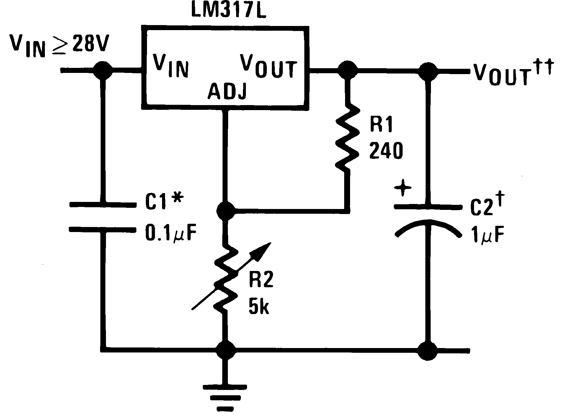
Schematic Diagram

†Optional—improves transient response
*Needed if device is more than 6 inches from filter capacitors

3 Description
The LM317L-N is an adjustable positive voltage regulator capable of supplying 100 mA over a 1.2-V to 37-V output range. The LM317L-N is easy to use and requires only two external resistors to set the output voltage. Both line and load regulation are better than standard fixed regulators. The LM317L-N is available packaged in a standard, easy-to-use
TO-92 transistor package.
The LM317L-N offers full overload protection. Included on the chip are current limit, thermal overload protection, and safe area protection. Normally, no capacitors are required unless the device is situated more than 6 inches from the input filter capacitors, in which case an input bypass is required.
The LM317L-N uses floating topology and sees only the input-to-output differential voltage, therefore supplies of several hundred volts can be regulated, provided the maximum input-to-output differential is not exceeded. The device makes a simple adjustable switching regulator, a programmable output regulator, or by connecting a fixed resistor between the adjustment and output, the LM317L-N can be used as a precision current regulator.
The LM317L-N is available in a standard 3-pin TO-92 transistor package, the 8-pin SOIC package, and 6-pin DSBGA package. The LM317L-N is rated for operation over a −40°C to 125°C range.
Device Information(1)
| PART NUMBER | PACKAGE | BODY SIZE (NOM) |
|---|---|---|
| LM317L-N | TO-92 (3) | 4.30 mm × 4.30 mm |
| SOIC (8) | 3.91 mm × 4.90 mm | |
| DSBGA (6) | 1.68 mm × 1.019 mm |
- For all available packages, see the orderable addendum at the end of the data sheet.