SNVS837B June 2013 – April 2016 LM3263
PRODUCTION DATA.
- 1 Features
- 2 Applications
- 3 Description
- 4 Revision History
- 5 Pin Configuration and Functions
- 6 Specifications
-
7 Detailed Description
- 7.1 Overview
- 7.2 Functional Block Diagram
- 7.3
Feature Description
- 7.3.1 PWM Operation
- 7.3.2 PFM Operation
- 7.3.3 Active Current Assist and Analog Bypass (ACB)
- 7.3.4 Bypass Operation
- 7.3.5 Dynamic Adjustment of Output Voltage
- 7.3.6 DC-DC Operating Mode Selection
- 7.3.7 Internal Synchronous Rectification
- 7.3.8 Current Limit
- 7.3.9 Timed Current Limit
- 7.3.10 Thermal Overload Protection
- 7.3.11 Start-Up
- 7.4 Device Functional Modes
- 7.5 Programming
- 7.6 Register Map
- 8 Application Information
- 9 Power Supply Recommendations
- 10Layout Considerations
- 11Device and Documentation Support
- 12Mechanical, Packaging, and Orderable Information
Package Options
Mechanical Data (Package|Pins)
- YFQ|16
Thermal pad, mechanical data (Package|Pins)
Orderable Information
1 Features
- MIPI® RFFE Digital Control Interface
- Operates from a Single Li-Ion Cell: 2.7 V to 5.5 V
- Dynamically Adjustable Output Voltage: 0.4 V to 3.6 V (Typical) in PFM and PWM Modes
- High-Efficiency PFM and PWM Modes With Internal Seamless Transition
- 2.5-A Maximum Load Current in PWM Mode
- 2.7 MHz (Typical) Switching Frequency
- ACB (Reduces Inductor Requirements and Size)
- Internal Compensation
- Current and Thermal Overload Protection
- Very Small Solution Size: Approximately 9.1 mm2
2 Applications
- Smartphones
- RF PC Cards
- Tablets, eBook Readers
- Handheld Radios
- Battery-Powered RF Devices
3 Description
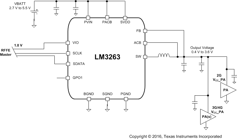
The LM3263 is a DC-DC converter optimized for powering multi-mode multi-band RF power amplifiers (PAs) from a single lithium-ion cell. The LM3263 steps down an input voltage from 2.7 V to 5.5 V to a dynamically adjustable output voltage of 0.4 V to 3.6 V. The output voltage is externally programmed through the RFFE Digital Control Interface and is set to ensure efficient operation at all power levels of the RF PA.
When operating in pulse width modulated (PWM) mode, the LM3263 produces a small and predictable amount of output voltage ripple thus meeting the power and stringent spectral-compliance needs of RF PAs with minimal filtering and minimal excess headroom. When operating in PFM mode, the LM3263 enables the lowest current consumption across PA output power level settings and therefore maximizes system efficiency.
The LM3263 has a unique Active Current assist and analog Bypass (ACB) feature to minimize inductor size without any loss of output regulation for the entire battery voltage and RF output power range, until dropout. ACB provides a parallel current path, when needed, to limit the maximum inductor current to 1.45 A (typical) while still driving a 2.5-A load. The ACB feature also enables operation with minimal dropout voltage.
Device Information(1)
| PART NUMBER | PACKAGE | BODY SIZE (MAX) |
|---|---|---|
| LM3263 | DSBGA (16) | 2.049 mm × 2.049 mm |
Typical Application
