SNOSC68C April   2012  – September 2015 LM3533

PRODUCTION DATA.  

  1. Features
  2. Applications
  3. Description
  4. Revision History
  5. Pin Configuration and Functions
  6. Specifications
    1. 6.1 Absolute Maximum Ratings
    2. 6.2 ESD Ratings
    3. 6.3 Recommended Operating Conditions
    4. 6.4 Thermal Information
    5. 6.5 Electrical Characteristics
    6. 6.6 I2C Timing Requirements
    7. 6.7 Typical Characteristics
  7. Detailed Description
    1. 7.1 Overview
    2. 7.2 Functional Block Diagram
    3. 7.3 Feature Description
      1. 7.3.1 Control Bank Mapping
        1. 7.3.1.1 High-Voltage Control Banks (A/B)
        2. 7.3.1.2 Low-Voltage Control Banks (C, D, E, And F)
      2. 7.3.2 Pattern Generator
      3. 7.3.3 Ambient Light Sensor Interface
      4. 7.3.4 PWM Input
      5. 7.3.5 HWEN Input
      6. 7.3.6 Thermal Shutdown
    4. 7.4 Device Functional Modes
      1. 7.4.1  High-Voltage Boost Converter
        1. 7.4.1.1 High-Voltage Current Sinks (HVLED1 And HVLED2)
        2. 7.4.1.2 High-Voltage Current String Biasing
        3. 7.4.1.3 Boost Switching-Frequency Select
      2. 7.4.2  Integrated Charge Pump
        1. 7.4.2.1 Charge Pump Disabled
        2. 7.4.2.2 Automatic Gain
        3. 7.4.2.3 Automatic Gain (Flying Capacitor Detection)
        4. 7.4.2.4 1× Gain
        5. 7.4.2.5 2× Gain
        6. 7.4.2.6 Low-Voltage Current Sinks (LVLED1 to LVLED5)
        7. 7.4.2.7 Low-Voltage LED Biasing
      3. 7.4.3  LED Current Mapping Modes
        1. 7.4.3.1 Exponential Mapping
        2. 7.4.3.2 Linear Mapping
      4. 7.4.4  LED Current Ramping
        1. 7.4.4.1 Start-Up/Shutdown Ramp
        2. 7.4.4.2 Run-Time Ramp
      5. 7.4.5  Brightness Register Current Control
      6. 7.4.6  PWM Control
        1. 7.4.6.1 PWM Input Frequency Range
        2. 7.4.6.2 PWM Input Polarity
      7. 7.4.7  ALS Current Control
        1. 7.4.7.1 ALS Brightness Zones (Zone Boundaries)
        2. 7.4.7.2 Zone Boundary Hysteresis
        3. 7.4.7.3 Zone Target Registers (ALSM1, ALSM2, ALSM3)
        4. 7.4.7.4 PWM Input in ALS Mode
      8. 7.4.8  ALS Functional Blocks
        1. 7.4.8.1  ALS Input
        2. 7.4.8.2  Analog Output Ambient Light Sensors (ALS Gain Setting Resistors)
        3. 7.4.8.3  PWM Output Ambient Light Sensors (Internal Filtering)
        4. 7.4.8.4  Internal 8-Bit ADC
        5. 7.4.8.5  ALS Averager
        6. 7.4.8.6  Initializing the ALS
        7. 7.4.8.7  ALS Algorithms
        8. 7.4.8.8  ALS Rules
        9. 7.4.8.9  Direct ALS Control
        10. 7.4.8.10 Up-Only Control
        11. 7.4.8.11 Down-Delay Control
      9. 7.4.9  Pattern Generator
        1. 7.4.9.1 Delay Time
        2. 7.4.9.2 Rise Time
        3. 7.4.9.3 Fall Time
        4. 7.4.9.4 High Period
        5. 7.4.9.5 Low Period
        6. 7.4.9.6 Low-Level Brightness
        7. 7.4.9.7 High-Level Brightness
        8. 7.4.9.8 ALS Controlled Pattern Current
        9. 7.4.9.9 Interrupt Output Mode
      10. 7.4.10 Fault Flags/Protection Features
        1. 7.4.10.1 Open LED String (HVLED)
        2. 7.4.10.2 Shorted LED String (HVLED)
        3. 7.4.10.3 Open LED (LVLED)
        4. 7.4.10.4 Shorted LED (LVLED)
        5. 7.4.10.5 Overvoltage Protection (Inductive Boost)
        6. 7.4.10.6 Current Limit (Inductive Boost)
        7. 7.4.10.7 Current Limit (Charge Pump)
    5. 7.5 Programming
      1. 7.5.1 I2C-Compatible Interface
        1. 7.5.1.1 Start and Stop Conditions
        2. 7.5.1.2 I2C-Compatible Address
        3. 7.5.1.3 Transferring Data
    6. 7.6 Register Maps
      1. 7.6.1 LM3533 Register Descriptions
        1. 7.6.1.1 Pattern Generator Registers
  8. Application and Implementation
    1. 8.1 Application Information
    2. 8.2 Typical Application
      1. 8.2.1 Design Requirements
      2. 8.2.2 Detailed Design Procedure
        1. 8.2.2.1 Boost Converter Maximum Output Power (Boost)
        2. 8.2.2.2 Peak Current Limited
        3. 8.2.2.3 Output Voltage Limited
        4. 8.2.2.4 Maximum Output Power (Charge Pump)
      3. 8.2.3 Application Curves
  9. Power Supply Recommendations
  10. 10Layout
    1. 10.1 Layout Guidelines
      1. 10.1.1 Boost
        1. 10.1.1.1 Boost Output Capacitor Selection and Placement
        2. 10.1.1.2 Schottky Diode Placement
        3. 10.1.1.3 Inductor Placement
        4. 10.1.1.4 Boost Input Capacitor Selection and Placement
      2. 10.1.2 Charge Pump
        1. 10.1.2.1 Flying Capacitor (CP)
        2. 10.1.2.2 Output Capacitor (CPOUT)
        3. 10.1.2.3 Charge Pump Input Capacitor Placement
    2. 10.2 Layout Example
  11. 11Device and Documentation Support
    1. 11.1 Device Support
      1. 11.1.1 Third-Party Products Disclaimer
    2. 11.2 Related Documentation
    3. 11.3 Community Resources
    4. 11.4 Trademarks
    5. 11.5 Electrostatic Discharge Caution
    6. 11.6 Glossary
  12. 12Mechanical, Packaging, and Orderable Information

Package Options

Mechanical Data (Package|Pins)
Thermal pad, mechanical data (Package|Pins)
Orderable Information

1 Features

  • Drives Two Parallel High-Voltage LED Strings for Display and Keypad Lighting
  • High-Voltage Strings Capable of up to 40-V Output Voltage and up to 90% Efficiency
  • Up to 30 mA per Current Sink (Both Backlight and Indicator)
  • 14-Bit Equivalent Exponential Dimming With 8-Bit Programmable Backlight Code
  • Selectable Analog ALS Input with 128 Programmable Gain-Setting Resistors or PWM ALS Input With Internal Low-Pass Filter
  • PWM Input for Content Adjustable Brightness Control
  • Five Low-Voltage Current Sinks for Indicator LEDs
  • Integrated Charge Pump for Improved Efficiency and VIN Operating Range
  • Internal Pattern Generation Engine
  • Fully Configurable LED Grouping and Control
  • Four Programmable Overvoltage Protection Thresholds (16 V, 24 V, 32 V, and 40 V)
  • Programmable 500-kHz and 1-MHz Switching Frequency
  • 27-mm2 Total Solution Size

2 Applications

  • Power Source for Smart Phone Illumination
  • Display, Keypad and Indicator Illumination
  • RGB Indicator Driver

3 Description

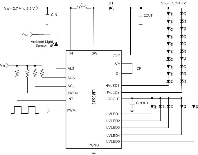
The LM3533 is a complete power source for backlight, keypad, and indicator LEDs in smartphone handsets. The high-voltage inductive boost converter provides the power for two series LED strings for display backlight and keypad functions (HVLED1 and HVLED2). The integrated charge pump provides the bias for the five low-voltage indicator LED current sinks (LVLED1 to LVLED5). All low-voltage current sinks can have a programmable pattern modulated onto their output current for a wide variety of blinking patterns.

Additional features include a pulse width modulation (PWM) control input for content adjustable backlight control (CABC), and an ambient light sensor interface (ALS) with an internal 8-bit ADC to provide automatic current adjustment based upon ambient light conditions. Both the PWM and ALS inputs can be used to control any high- or low-voltage current sink.

The LM3533 is fully programmable via an I2C-compatible interface. The device is available in a
20-pin DSBGA and operates over a 2.7-V to 5.5-V input voltage range and a −40°C to +85°C temperature range.

Device Information(1)

PART NUMBER PACKAGE BODY SIZE (MAX)
LM3533 DSBGA (20) 2.04 mm × 1.78 mm
  1. For all available packages, see the orderable addendum at the end of the data sheet.

Typical Application Circuit
LM3533 30135701.gif