-
LM3559 Synchronous Boost Flash Driver With Dual 900-mA High-Side Current Sources (1.8-A Total Flash Current)
- 1 Features
- 2 Applications
- 3 Description
- 4 Revision History
- 5 Pin Configuration and Functions
- 6 Specifications
- 7 Typical Characteristics
-
8 Detailed Description
- 8.1 Overview
- 8.2 Functional Block Diagram
- 8.3
Feature Description
- 8.3.1 Power Amplifier Synchronization (TX1)
- 8.3.2 Input Voltage Flash Monitor Fault
- 8.3.3 Independent LED Control
- 8.3.4 Hardware Torch
- 8.3.5 Fault Protections
- 8.3.6 Input Voltage (VIN ) Monitor
- 8.3.7 VIN Flash Monitor (Flash Current Rising)
- 8.3.8 Last Flash Register
- 8.3.9 LED Voltage Monitor
- 8.3.10 ADC Delay
- 8.3.11 Flags Register and Fault Indicators
- 8.4
Device Functional Modes
- 8.4.1 Start-Up (Enabling the Device)
- 8.4.2 Pass Mode
- 8.4.3 Flash Mode
- 8.4.4 Torch Mode
- 8.4.5 Privacy-Indicate Mode
- 8.4.6 GPIO1 Mode
- 8.4.7 TX2/INT/GPIO2
- 8.4.8 TX2 Mode
- 8.4.9 GPIO2 Mode
- 8.4.10 Interrupt Output (INT Mode)
- 8.4.11 NTC Mode
- 8.4.12 Alternate External Torch (AET Mode)
- 8.4.13 Automatic Conversion Mode
- 8.4.14 Manual Conversion Mode
- 8.5 Programming
- 8.6
Register Maps
- 8.6.1 Enable Register
- 8.6.2 Torch Brightness Register
- 8.6.3 Flash Brightness Register
- 8.6.4 Flash Duration Register
- 8.6.5 Flags Register
- 8.6.6 Configuration Register 1
- 8.6.7 Configuration Register 2
- 8.6.8 GPIO Register
- 8.6.9 Last Flash Register
- 8.6.10 VLED Monitor Register
- 8.6.11 ADC Delay Register
- 8.6.12 Input Voltage Monitor Register
- 8.6.13 Privacy Register
- 8.6.14 Privacy PWM Period Register
- 8.6.15 Indicator Register
- 8.6.16 Indicator Blinking Register
- 9 Application and Implementation
- 10Power Supply Recommendations
- 11Layout
- 12Device and Documentation Support
- 13Mechanical, Packaging, and Orderable Information
- IMPORTANT NOTICE
Package Options
Mechanical Data (Package|Pins)
- YZR|16
Thermal pad, mechanical data (Package|Pins)
Orderable Information
LM3559 Synchronous Boost Flash Driver With Dual 900-mA High-Side Current Sources (1.8-A Total Flash Current)
1 Features
- Dual High-Side Current Sources Allow for Grounded Cathode LED Operation
- Accurate and Programmable LED Current from 28.125 mA to 1.8 A
- Optimized Flash Current During Low Battery Conditions
- Independent LED Current Source Programmability
- Four Operating Modes: Torch, Flash, Privacy Indicate, and Message Indicator
- 4-Bit Analog-to-Digital (ADC) for VLED Monitoring
- Battery Voltage Sensing and Current Scale-Back
- LED Sensing and Current Scale-Back
- Hardware Flash and Torch Enable
- Active-Low Hardware Reset
- Dual Synchronization Inputs for RF Power Amplifier Pulse Events
- LED and Output Disconnect During Shutdown
- Open and Short LED Detection
- 400-kHz I2C-Compatible Interface
2 Applications
- Camera Phone LED Flash
- White LED Biasing
Simplified Schematic

3 Description
The LM3559 is a 2-MHz fixed-frequency synchronous boost converter with two 900-mA constant current drivers for high-current white LEDs. The dual high-side current sources allow for grounded cathode LED operation and can be tied together for providing flash currents of up to 1.8 A. An adaptive regulation method ensures the current for each LED remains in regulation and maximizes efficiency.
The LM3559 is controlled via an I2C-compatible interface. Features include: an internal 4-bit ADC to monitor the LED voltage, independent LED current control, a hardware flash enable allowing a logic input to trigger the flash pulse, dual TX inputs which force the flash pulse into a low-current torch mode allowing for synchronization to RF power amplifier events or other high-current conditions, an integrated comparator designed to monitor an NTC thermistor and provide an interrupt to the LED current, an input voltage monitor to monitor low battery conditions, and a flash current scale-back feature that actively monitors the battery voltage and optimizes the flash current during low battery-voltage conditions. Additionally, an active high HWEN input provides a hardware shutdown during system software failures.
The 2-MHz switching frequency, overvoltage protection, and adjustable current limit allow for the use of tiny, low-profile (1-µH or 2.2-µH) inductors and (10-µF) ceramic capacitors. The device is available in a ultra-small 16-pin DSBGA package (total solution size < 26 mm2) and operates over the –40°C to +85°C temperature range.
Device Information(1)
| PART NUMBER | PACKAGE | BODY SIZE (NOM) |
|---|---|---|
| LM3559 | DSBGA (16) | 1.96 mm × 1.96 mm |
- For all available packages, see the orderable addendum at the end of the data sheet.
LED Efficiency vs VIN Dual LEDs

4 Revision History
Changes from A Revision (May 2013) to B Revision
- Added Device Information and Pin Configuration and Functions sections, ESD Ratings and Thermal Information tables, Feature Description, Device Functional Modes, Application and Implementation, Power Supply Recommendations, Layout, Device and Documentation Support, and Mechanical, Packaging, and Orderable Information sectionsGo
- Added Thermal Information table with revised RθJA value (from "50.4°C/W" to "71.3°C/W") and additional thermal values. Go
Changes from * Revision (May 2013) to A Revision
- Changed layout of National Data Sheet to TI formatGo
5 Pin Configuration and Functions
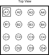
Pin Functions
| PIN | TYPE | DESCRIPTION | |
|---|---|---|---|
| NO. | NAME | ||
| A1 | LED1 | Power | High-side current source output for flash LED1 |
| A2, B2 | OUT | Power | Step-up DC-DC converter output. Connect a 10-µF ceramic capacitor between this pin and GND. |
| A3, B3 | SW | Power | Drain connection for internal NMOS and synchronous PMOS switches |
| A4, B4 | GND | Ground | Ground |
| B1 | LED2 | Output | High-side current source output for flash LED2 |
| C1 | LEDI/NTC | Input/Output | Configureable as a high-side current source output for indicator LED or comparator input for LED temperature sensing |
| C2 | TX1/TORCH/GPIO1 | Input/Output | Configureable as a dual-polarity RF power amplifier synchronization input, a hardware torch mode enable, or as a general purpose logic I/O. This pin has an internal 300-kΩ pulldown to GND. |
| C3 | STROBE | Input | Active high hardware flash enable. Drive STROBE high to turn on the flash current pulse. This pin has an internal 300-kΩ pulldown to GND. |
| C4 | IN | Power | Input voltage connection. Connect IN to the input supply, and bypass to GND with a minimum 10-µF or larger ceramic capacitor. |
| D1 | TX2/INT/GPIO2 | Input/Output | Configurable as a dual-polarity power amplifier synchronization input, an interrupt output, or as a general purpose logic I/O. This pin has an internal 300-kΩ pulldown to GND. |
| D2 | SDA | Input/Output | Serial data input output. High impedance in shutdown or in power down. |
| D3 | SCL | Input | Serial clock input. High impedance in shutdown or in power down. |
| D4 | HWEN | Input | Logic high hardware enable. HWEN is a high impedance input and is normally connected with an external pullup resistor to a logic high voltage. |
6 Specifications
6.1 Absolute Maximum Ratings
over operating free-air temperature range (unless otherwise noted)(1)| MIN | MAX | UNIT | ||
|---|---|---|---|---|
| VIN | –0.3 | 6 | V | |
| VSCL, VSDA, VHWEN, VSTROBE, VTX1, VTX2, VLED1, VLED2, VLEDI/NTC | –0.3 | to the lesser of (VIN + 0.3 V) with 6 V maximum | V | |
| VSW, VOUT | –0.3 | 6 | V | |
| Continuous power dissipation(2) | Internally limited | |||
| Junction temperature, TJ-MAX | 150 | °C | ||
| Storage temperature, Tstg | –65 | 150 | °C | |
6.2 ESD Ratings
| VALUE | UNIT | |||
|---|---|---|---|---|
| V(ESD) | Electrostatic discharge | Human-body model (HBM), per ANSI/ESDA/JEDEC JS-001(1) | ±2000 | V |
6.3 Recommended Operating Conditions
over operating free-air temperature range (unless otherwise noted)| MIN | MAX | UNIT | ||
|---|---|---|---|---|
| Input voltage, VIN | 2.5 | 5.5 | V | |
| Junction temperature, TJ | –40 | 125 | °C | |
| Ambient temperature, TA(1) | –40 | 85 | °C | |
6.4 Thermal Information
| THERMAL METRIC(1) | LM3559 | UNIT | |
|---|---|---|---|
| YZR (DSBGA) | |||
| 16 PINS | |||
| RθJA | Junction-to-ambient thermal resistance(2) | 71.3 | °C/W |
| RθJC(top) | Junction-to-case (top) thermal resistance | 18.4 | °C/W |
| RθJB | Junction-to-board thermal resistance | 9.8 | °C/W |
| ψJT | Junction-to-top characterization parameter | 1.7 | °C/W |
| ψJB | Junction-to-board characterization parameter | 1.7 | °C/W |
| RθJC(bot) | Junction-to-case (bottom) thermal resistance | 9.7 | °C/W |
6.5 Electrical Characteristics
Unless otherwise specified, VIN = 3.6 V, VHWEN = VIN, TA = 25°C.(1) (2)| PARAMETER | TEST CONDITIONS | MIN | TYP | MAX | UNIT | |||
|---|---|---|---|---|---|---|---|---|
| CURRENT SOURCE SPECIFICATIONS | ||||||||
| ILED | Current source accuracy | ILED1 + ILED2, 3 V ≤ VIN ≤ 4.2 V, VOUT = 4.5 V | 900-mA flash current setting, per current source | –7% | 1800 | 7% | mA | |
| 900-mA flash current setting, per current source –40°C ≤ TA ≤ 85°C |
–4% | 1800 | 4% | |||||
| 28.125-mA torch current, per current source | –10% | 56.2 | 10% | |||||
| 28.125-mA torch current, per current source –40°C ≤ TA ≤ 85°C |
||||||||
| VOUT – VLED1/2 | Current source regulation voltage | ILED = 1.8 A (ILED1 + ILED2), VOUT = 4.5 V | 270 | mV | ||||
| VOVP | Output overvoltage protection trip point(3) | ON threshold | 5 | V | ||||
| ON threshold, –40°C ≤ TA ≤ 85°C | 4.925 | 5.075 | ||||||
| OFF threshold | 4.88 | |||||||
| STEP-UP DC-DC CONVERTER SPECIFICATIONS | ||||||||
| RPMOS | PMOS switch on-resistance | IPMOS = 1A | 80 | mΩ | ||||
| RNMOS | NMOS switch on-resistance | INMOS = 1A | 80 | mΩ | ||||
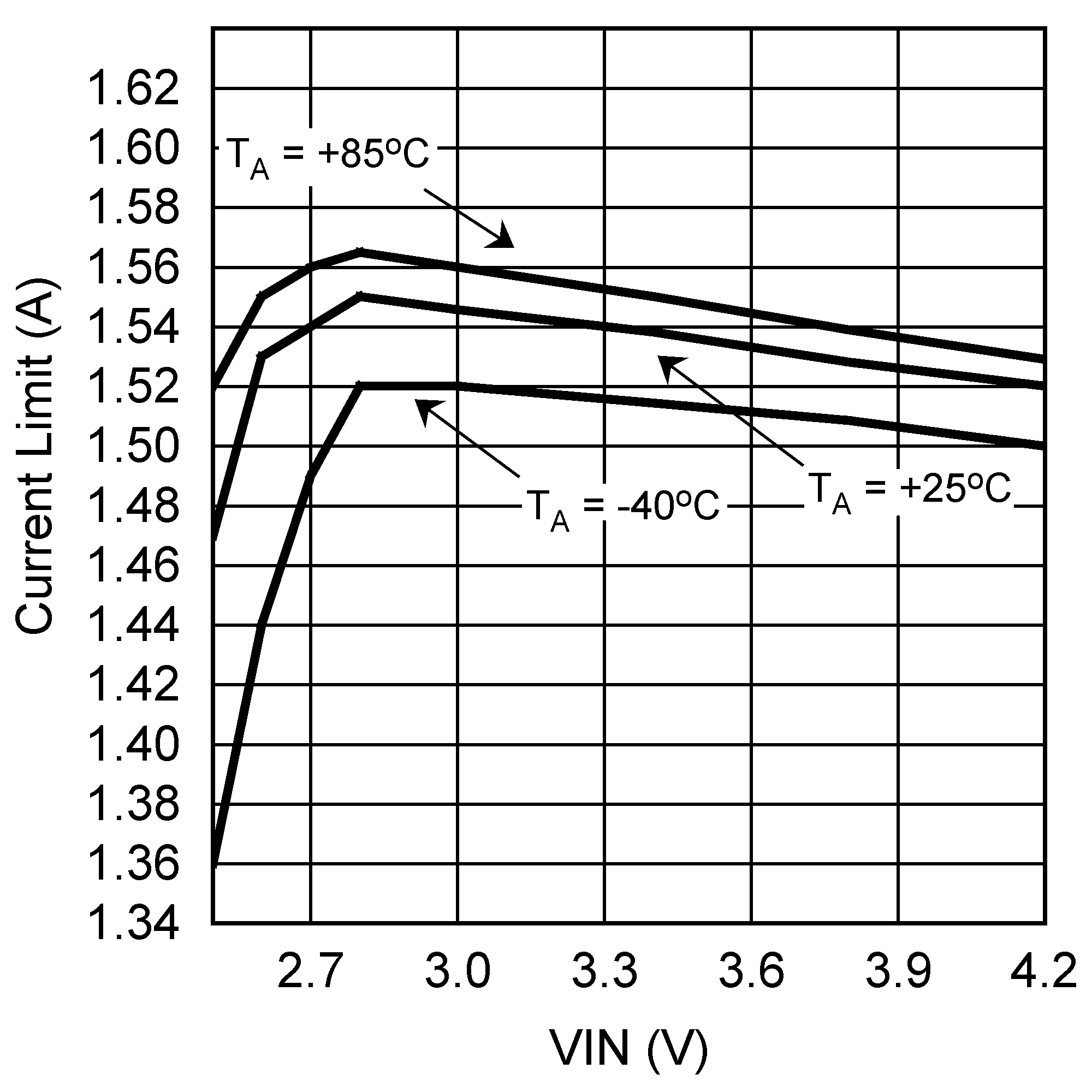
| ICL | Switch current limit(4) | 3 V ≤ VIN ≤ 4.2 V | Flash Duration Register bits [6:5] = 00 | 1.4 | A | |||
| 3 V ≤ VIN ≤ 4.2 V –40°C ≤ TA ≤ 85°C |
1.2 | 1.6 | ||||||
| 3 V ≤ VIN ≤ 4.2 V | Flash Duration Register bits [6:5] = 01 | 2.1 | ||||||
| 3 V ≤ VIN ≤ 4.2 V –40°C ≤ TA ≤ 85°C |
1.8 | 2.3 | ||||||
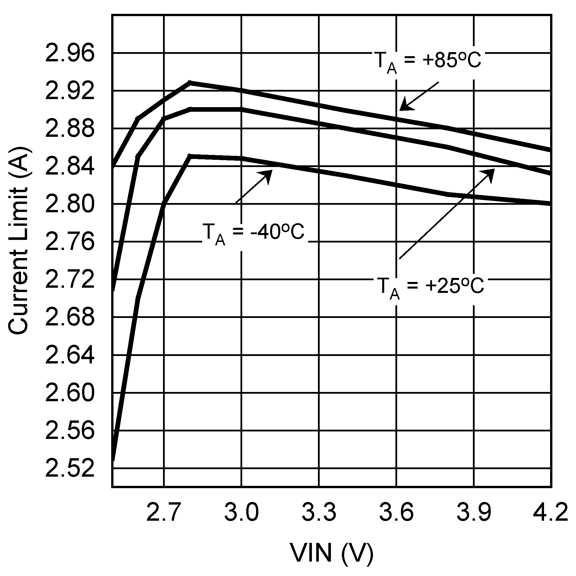
| 3 V ≤ VIN ≤ 4.2 V | Flash Duration Register bits [6:5] = 10 | 2.7 | ||||||
| 3 V ≤ VIN ≤ 4.2 V –40°C ≤ TA ≤ 85°C |
2.4 | 3 | ||||||
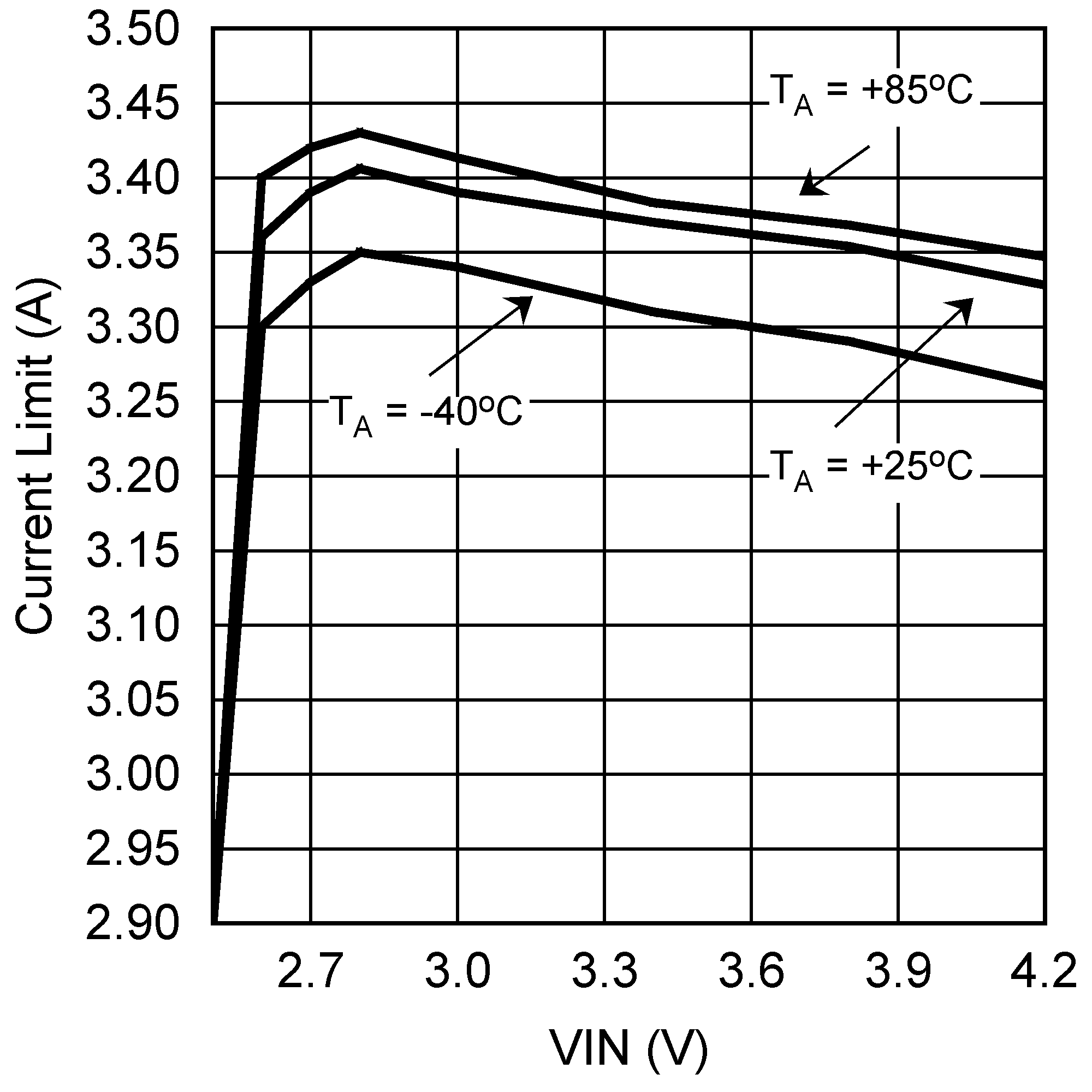
| 3 V ≤ VIN ≤ 4.2 V | Flash Duration Register bits [6:5] = 11 | 3.2 | ||||||
| 3 V ≤ VIN ≤ 4.2 V –40°C ≤ TA ≤ 85°C |
2.9 | 3.5 | ||||||
| IOUT_SC | Output short-circuit current limit | VOUT < 2.3 V | 350 | mA | ||||
| ILEDI/NTC | Indicator current | Register 0x12, bits[2:0] = 111, 2.7 V ≤ VIN ≤ 4.2 V VLEDI/NTC = 2 V, –40°C ≤ TA ≤ 85°C |
18 | mA | ||||
| Register 0x12, bits[2:0] = 111, 2.7 V ≤ VIN ≤ 4.2 V VLEDI/NTC = 2 V |
16 | 20 | ||||||
| VTRIP | Comparator trip threshold | Configuration register 1, bit [4] = 1, 3 V ≤ VIN ≤ 4.2 V |
1 | V | ||||
| Configuration register 1, bit [4] = 1, 3 V ≤ VIN ≤ 4.2 V, –40°C ≤ TA ≤ 85°C |
0.97 | 1.03 | ||||||
| ƒSW | Switching frequency | 2.7 V ≤ VIN ≤ 5.5 V | 2 | MHz | ||||
| 2.7 V ≤ VIN ≤ 5.5 V, –40°C ≤ TA ≤ 85°C | 1.8 | 2.2 | ||||||
| IQ | Quiescent supply current | Device not switching, VOUT = 3V | 650 | µA | ||||
| Device switching, VOUT = 4.5V | 1.55 | mA | ||||||
| Indicate mode, Indicator Register bits [2:0] = 111 VLEDI/NTC = 2 V |
590 | µA | ||||||
| Indicate mode, Indicator Register bits [2:0] = 111 VLEDI/NTC = 2 V, –40°C ≤ TA ≤ 85°C |
750 | |||||||
| ISHDN | Shutdown supply current | 2.7 V ≤ VIN ≤ 5.5 V, –40°C ≤ TA ≤ 85°C | HWEN = GND | 1 | µA | |||
| ISTBY | Standby supply current | 2.7 V ≤ VIN ≤ 5.5 V | HWEN = VIN, Enable Register bits [1:0] = 00 | 1.25 | µA | |||
| 2.7 V ≤ VIN ≤ 5.5 V, –40°C ≤ TA ≤ 85°C | 2.4 | |||||||
| VIN_TH | VIN monitor threshold | VIN Monitor Register = 0x01 | 2.9 | V | ||||
| VIN Monitor Register = 0x01, –40°C ≤ TA ≤ 85°C | 2.85 | 2.95 | ||||||
| VIN_FLASH_TH | VIN flash monitor threshold | VIN Monitor Register = 0x08 | 2.9 | V | ||||
| VIN Monitor Register = 0x08, –40°C ≤ TA ≤ 85°C | 2.85 | 2.95 | ||||||
| tTX | Flash-to-torch LED current settling time | TX_ Low to High ILED1 + ILED2 = 1.8A to 112.5mA |
20 | µs | ||||
| tD | Time from when ILED hits target until VLED data is available | ADC Delay Register bit [5] = 1 | 16 | µs | ||||
| ADC Delay Register bit [5] = 0 ADC Delay Register bits [4:0] = 0000 |
250 | |||||||
| VF_ADC | ADC threshold | VLED Monitor Register bits [3:0] = 1111 | 4.6 | V | ||||
| VLED Monitor Register bits [3:0] = 1111 –40°C ≤ TA ≤ 85°C |
4.4 | 4.8 | ||||||
| HWEN, STROBE, TX1/TORCH/GPIO1, TX2/INT/GPIO2 VOLTAGE SPECIFICATIONS | ||||||||
| VIL | Input logic low | 2.7 V ≤ VIN ≤ 5.5 V, –40°C ≤ TA ≤ 85°C | 0 | 0.4 | V | |||
| VIH | Input logic high | 2.7 V ≤ VIN ≤ 5.5 V, –40°C ≤ TA ≤ 85°C | 1.2 | VIN | V | |||
| RPD | Internal pulldown resistance on TX1, TX2, STROBE | 300 | kΩ | |||||
| I2C-COMPATIBLE VOLTAGE SPECIFICATIONS (SCL, SDA) | ||||||||
| VIL | Input logic low | 2.7 V ≤ VIN ≤ 5.5 V, –40°C ≤ TA ≤ 85°C | 0 | 0.4 | V | |||
| VIH | Input logic high | 2.7 V ≤ VIN ≤ 5.5 V | 1.3 | VIN | V | |||
| VOL | Output logic low (SDA) | ILOAD = 3 mA 2.7 V ≤ VIN ≤ 5.5 V, –40°C ≤ TA ≤ 85°C |
0.4 | V | ||||
6.6 I2C Timing Requirements (SCL, SDA)
See(1)| MIN | NOM | MAX | UNIT | ||
|---|---|---|---|---|---|
| 1/t1 | SCL(clock frequency) | 400 | kHz | ||
| t2 | Data in setup time to SCL high | 100 | ns | ||
| t3 | Data out stable after SCL low | 0 | ns | ||
| t4 | SDA low setup time to SCL low (start) | 100 | ns | ||
| t5 | SDA high hold time after SCL high (stop) | 100 | ns | ||
7 Typical Characteristics
Unless otherwise specified: VIN = 3.6 V, COUT = 10 µF, CIN = 10 µF, L = 1 µH (TOKO FDSD0312-1R0, RL = 43 mΩ), Figure 43.
| Enable Register = 0x18 | ||
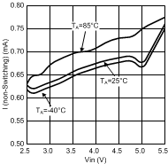

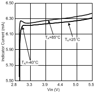
| Register Bits [2:0] = 0x02 | ||

| Upper 5 Flash Brightness Codes | ||

| Upper 4 Torch Brightness Codes | ||
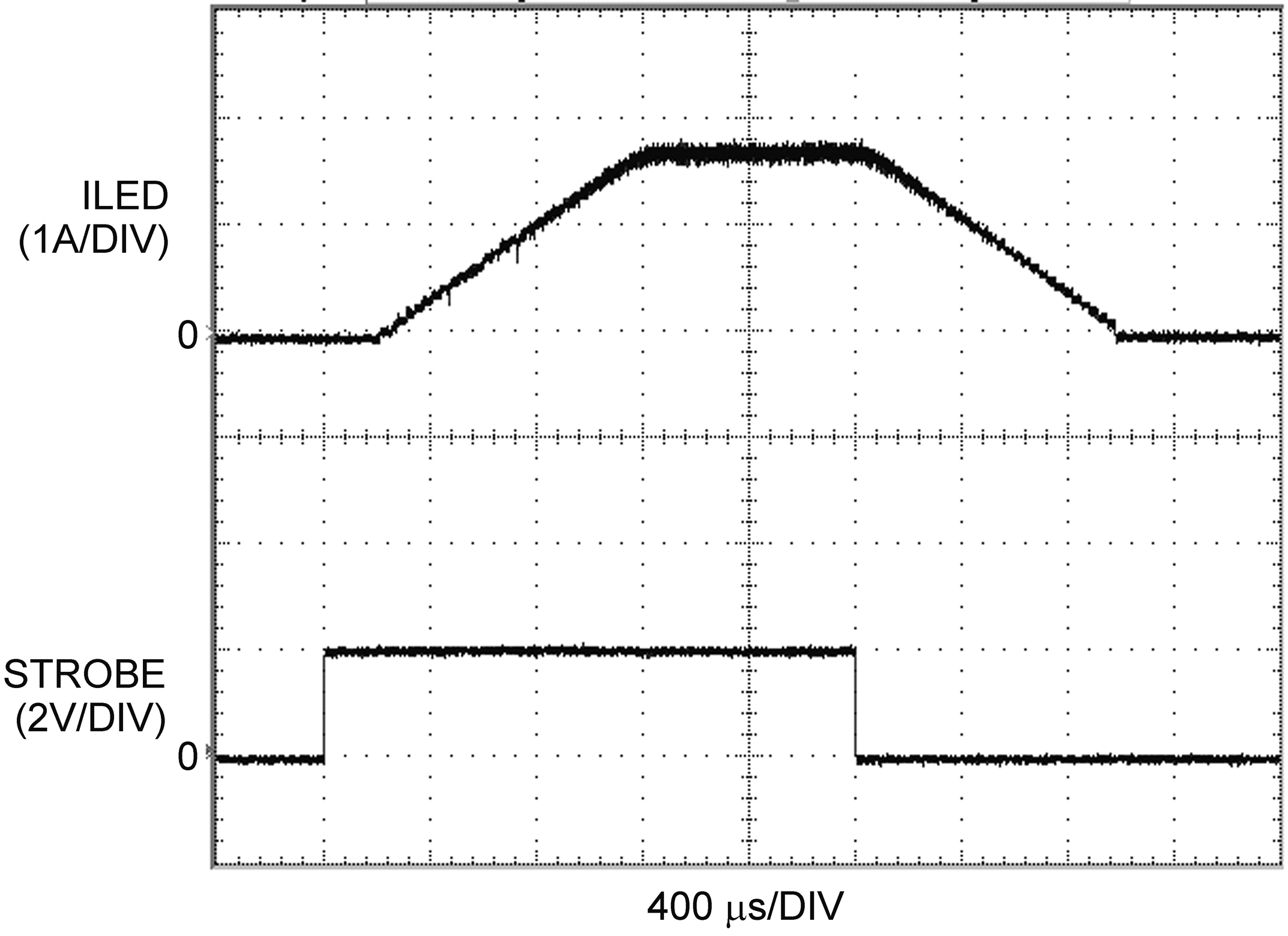

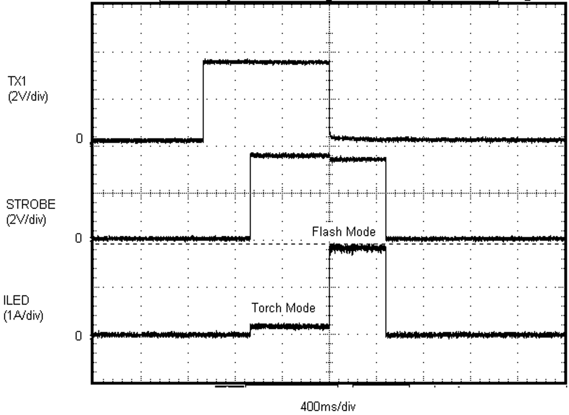


| VHWEN= 0 V |
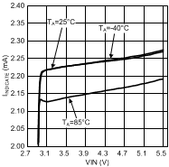
| Register Bits [2:0] = 0x00 | ||

| Register Bits [2:0] = 0x07 | ||
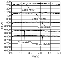
| Middle 5 Flash Brightness Codes | ||

| Lower 4 Torch Brightness Codes | ||

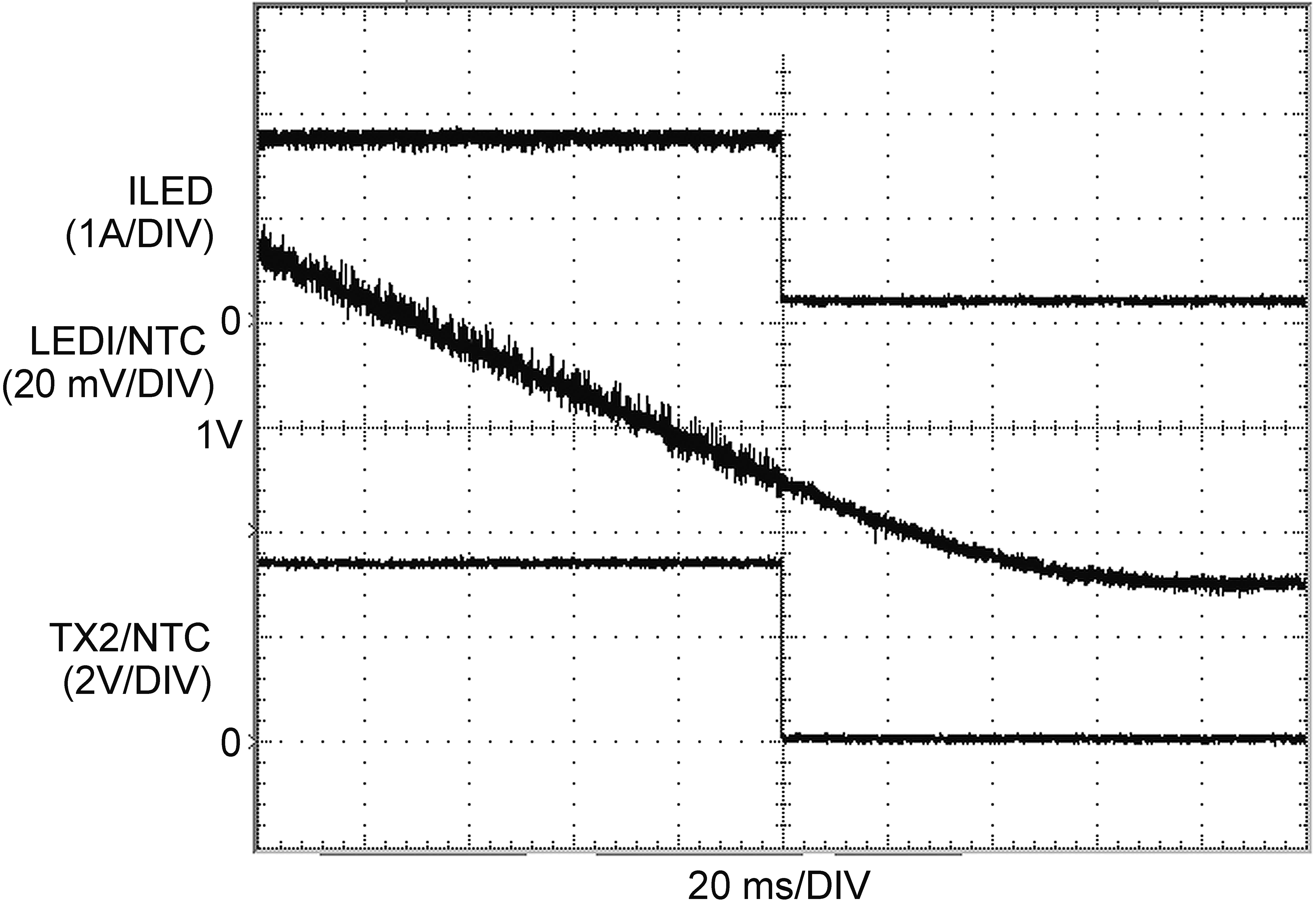
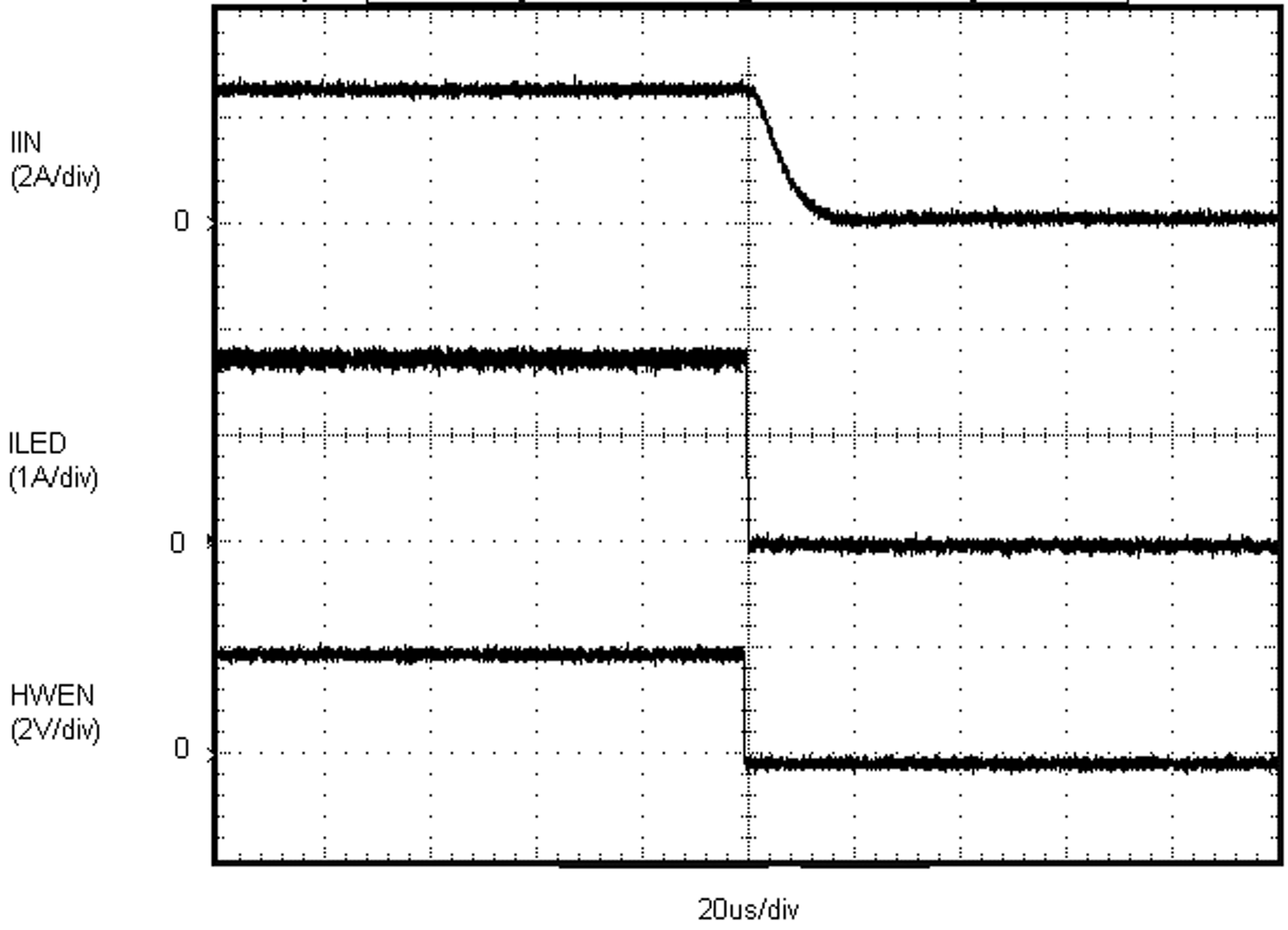

| TX2 Active High |
