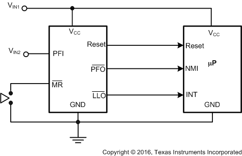
The LM3704 is a feature-rich, easy-to-use voltage supervisor. It is offered in both push-pull and open-drain configuration with a tight 2% accuracy over temperature.
The LM3704 features include a manual reset, low-line output, and power-fail input detection. The power-fail input allows for a configurable second rail to be monitored helping detect upstream failures. The low-line output is used as a second interrupt line to indicate a fall in VCC (1.02 × VRST).
PART NUMBER | PACKAGE | BODY SIZE (NOM) |
---|---|---|
LM3704 | VSSOP (10) | 3.00 mm × 3.00 mm |
PIN | I/O | DESCRIPTION | |
---|---|---|---|
NO. | NAME | ||
1 | VCC | I | Power supply input. |
2 | MR | I | Manual-reset input. When MR is less than VMRT (manual reset threshold) RESET/RESET is engaged. |
3 | PFI | I | Power-fail comparator input. When PFI is less than VPFT (power-fail reset threshold), the PFO goes low. Otherwise, PFO remains high. |
4 | NC | — | No connection. |
5 | GND | — | Ground reference for all signals. |
6 | NC | — | No connection. |
7 | LLO | O | Low-line logic output. Early power-fail warning output. Low when VCC falls below VLLOT (low-line output threshold). This output can be used to generate an NMI (non-maskable interrupt) to provide an early warning of imminent power failure. |
8 | PFO | O | Power-fail logic output. When PFI is below VPFT, PFO goes low; otherwise, PFO remains high. |
9 | NC | — | No connection. Test input used at factory only. Leave floating. |
10 | RESET | O | Reset logic output. Pulses low for tRP (reset time-out period) when triggered, and stays low whenever VCC is below the reset threshold or when MR is below VMRT. It remains low for tRP after either VCC rises above the reset threshold, or after MR input rises above VMRT. |
MIN | MAX | UNIT | ||
---|---|---|---|---|
Supply voltage, VCC | –0.3 | 6 | V | |
All other inputs | –0.3 | VCC + 0.3 | V | |
Power dissipation | See(2) | |||
Storage temperature, Tstg | –65 | 150 | °C |
VALUE | UNIT | |||
---|---|---|---|---|
V(ESD) | Electrostatic discharge | Human-body model (HBM), per ANSI/ESDA/JEDEC JS-001(1) | ±1500 | V |
Charged-device model (CDM), per JEDEC specification JESD22-C101(2) | ±150 |
MIN | MAX | UNIT | ||
---|---|---|---|---|
TA | Free-air temperature | –40 | 85 | °C |
THERMAL METRIC(1) | LM3704 | UNIT | |
---|---|---|---|
DGS (VSSOP) | |||
10 PINS | |||
RθJA | Junction-to-ambient thermal resistance | 163.7 | °C/W |
RθJC(top) | Junction-to-case (top) thermal resistance | 58.3 | °C/W |
RθJB | Junction-to-board thermal resistance | 83.5 | °C/W |
ψJT | Junction-to-top characterization parameter | 6 | °C/W |
ψJB | Junction-to-board characterization parameter | 82.2 | °C/W |
RθJC(bot) | Junction-to-case (bottom) thermal resistance | — | °C/W |
PARAMETER | TEST CONDITIONS | MIN | TYP | MAX | UNIT | ||
---|---|---|---|---|---|---|---|
POWER SUPPLY | |||||||
VCC | Operating voltage | LM3704, TJ = –40°C to 85°C | 1 | 5.5 | V | ||
ICC | VCC supply current | All inputs = VCC, all outputs floating |
TJ = 25°C | 28 | µA | ||
TJ = –40°C to 85°C | 50 | ||||||
RESET THRESHOLD | |||||||
VRST | Reset threshold | VCC falling | TJ = 25°C | –0.5% | VRST | 0.5% | |
TJ = –40°C to 85°C | –2% | 2% | |||||
TJ = 0°C to 70°C | –1.5% | 1.5% | |||||
VRSTH | Reset threshold hysteresis | 0.0032 × VRST | mV | ||||
tRP | Reset time-out period | Reset time-out period = C | TJ = 25°C | 200 | ms | ||
TJ = –40°C to 85°C | 140 | 280 | |||||
tRD | VCC to reset delay | VCC falling at 1 mV/µs | 20 | µs | |||
RESET | |||||||
VOL | RESET | VCC > 1.0 V, ISINK = 50 µA, TJ = –40°C to 85°C |
0.3 | V | |||
VCC > 1.2 V, ISINK = 100 µA, TJ = –40°C to 85°C |
0.3 | ||||||
VCC > 2.25 V, ISINK = 900 µA, TJ = –40°C to 85°C |
0.3 | ||||||
VCC > 2.7 V, ISINK = 1.2 mA, TJ = –40°C to 85°C |
0.3 | ||||||
VCC > 4.5 V, ISINK = 3.2 mA, TJ = –40°C to 85°C |
0.4 | ||||||
VOH | RESET | VCC > 2.25 V, ISOURCE = 300 µA, TJ = –40°C to 85°C |
0.8 × VCC | V | |||
VCC > 2.7 V, ISOURCE = 500 µA, TJ = –40°C to 85°C |
0.8 × VCC | ||||||
VCC > 4.5 V, ISOURCE = 800 µA, TJ = –40°C to 85°C |
VCC − 1.5 | ||||||
PFI/MR | |||||||
VPFT | PFI input threshold | TJ = 25°C | 1.225 | V | |||
TJ = –40°C to 85°C | 1.2 | 1.25 | |||||
VMRT | MR Input threshold | TJ = –40°C to 85°C | MR, low | 0.8 | V | ||
MR, high | 2 | ||||||
VPFTH/ VMRTH |
PFI/MR threshold hysteresis | PFI/MR falling, VCC = VRST MAX to 5.5 V | 0.0032 × VRST | mV | |||
IPFI | Input current (PFI only) | TJ = –40°C to 85°C | –75 | 75 | nA | ||
RMR | MR pullup resistance | TJ = 25°C | 56 | kΩ | |||
TJ = –40°C to 85°C | 35 | 75 | |||||
tMD | MR to reset delay | 12 | µS | ||||
tMR | MR pulse width | TJ = –40°C to 85°C | 25 | µS | |||
PFO, LLO | |||||||
VOL | PFO, LLO output low voltage | VCC > 2.25 V, ISINK = 900 µA, TJ = –40°C to 85°C |
0.3 | V | |||
VCC > 2.7 V, ISINK = 1.2 mA, TJ = –40°C to 85°C |
0.3 | ||||||
VCC > 4.5 V, ISINK = 3.2 mA, TJ = –40°C to 85°C |
0.4 | ||||||
VOH | PFO, LLO output high voltage | VCC > 2.25 V, ISOURCE = 300 µA, TJ = –40°C to 85°C |
0.8 VCC | V | |||
VCC > 2.7 V, ISOURCE = 500 µA, TJ = –40°C to 85°C |
0.8 VCC | ||||||
VCC > 4.5 V, ISOURCE = 800 µA, TJ = –40°C to 85°C |
VCC − 1.5 | ||||||
LLO OUTPUT | |||||||
VLLOT | LLO output threshold | VLLO − VRST, VCC falling | TJ = 25°C | 1.02 × VRST | V | ||
TJ = –40°C to 85°C | 1.01 × VRST | 1.03 × VRST | |||||
VLLOTH | Low-line comparator hysteresis | 0.0032 × VRST | mV | ||||
tCD | Low-line comparator delay | VCC falling at 1 mV/µs | 20 | µs |
VCC = 3.3 V |