-
LM5010A, LM5010A-Q1 High-Voltage 1-A Step-Down Switching Regulator
- 1 Features
- 2 Applications
- 3 Description
- 4 Revision History
- 5 Pin Configuration and Functions
- 6 Specifications
- 7 Detailed Description
- 8 Application and Implementation
- 9 Power Supply Recommendations
- 10Layout
- 11Device and Documentation Support
- 12Mechanical, Packaging, and Orderable Information
- IMPORTANT NOTICE
Package Options
Mechanical Data (Package|Pins)
- PWP|14
Thermal pad, mechanical data (Package|Pins)
- PWP|14
Orderable Information
LM5010A, LM5010A-Q1 High-Voltage 1-A Step-Down Switching Regulator
1 Features
- LM5010A-Q1 Qualified for Automotive Applications
- AEC-Q100 Qualified With the Following Results:
- Device Temperature Grade 1: –40°C to 125°C Ambient Operating Temperature Range
- Device Temperature Grade 0: –40°C to 150°C Ambient Operating Temperature Range
- Device HBM ESD Classification Level 2
- Device CDM ESD Classification Level C5
- Wide 6-V to 75-V Input Voltage Range
- Valley Current Limit at 1.25 A
- Programmable Switching Frequency Up To 1 MHz
- Integrated 80-V N-Channel Buck Switch
- Integrated High Voltage Bias Regulator
- No Loop Compensation Required
- Ultra-Fast Transient Response
- Nearly Constant Operating Frequency With Line and Load Variations
- Adjustable Output Voltage
- 2.5-V, ±2% Feedback Reference
- Programmable Soft-Start
- Thermal Shutdown
- Exposed Thermal Pad for Improved Heat Dissipation
2 Applications
- Non-Isolated Telecommunications Regulators
- Secondary Side Post Regulators
- Automotive Electronics
3 Description
The LM5010Ax step-down switching regulator is an enhanced version of the LM5010 with the input operating range extended to 6-V minimum. The LM5010Ax features all the functions needed to implement a low-cost, efficient, buck regulator capable of supplying in excess of 1-A load current. This high-voltage regulator integrates an N-Channel Buck Switch, and is available in thermally enhanced 10-pin WSON and 14-pin HTSSOP packages. The constant ON-time regulation scheme requires no loop compensation resulting in fast load transient response and simplified circuit implementation. The operating frequency remains constant with line and load variations due to the inverse relationship between the input voltage and the ON-time. The valley current limit detection is set at 1.25 A. Additional features include: VCC undervoltage lockout, thermal shutdown, gate drive undervoltage lockout, and maximum duty cycle limiter.
Device Information(1)
| PART NUMBER | PACKAGE | BODY SIZE (NOM) |
|---|---|---|
| LM5010Ax | WSON (10) | 4.00 mm × 4.00 mm |
| HTSSOP (14) | 4.40 mm × 5.00 mm |
- For all available packages, see the orderable addendum at the end of the data sheet.
Basic Step-Down Regulator

4 Revision History
Changes from E Revision (February 2013) to F Revision
- Added ESD Ratings table, Feature Description section, Device Functional Modes, Application and Implementation section, Power Supply Recommendations section, Layout section, Device and Documentation Support section, and Mechanical, Packaging, and Orderable Information sectionGo
Changes from D Revision (February 2013) to E Revision
- Changed layout of National Data Sheet to TI formatGo
5 Pin Configuration and Functions
Pin Functions
| PIN | I/O | DESCRIPTION | ||
|---|---|---|---|---|
| NAME | WSON | HTSSOP | ||
| BST | 2 | 3 | I | Boost pin for bootstrap capacitor: Connect a capacitor from SW to the BST pin. The capacitor is charged from VCC through an internal diode during the buck switch OFF-time. |
| EP | — | — | — | Exposed pad |
| FB | 6 | 9 | I | Voltage feedback input from the regulated output: Input to both the regulation and overvoltage comparators. The FB pin regulation level is 2.5 V. |
| ISEN | 3 | 4 | I | Current sense: During the buck switch OFF-time, the inductor current flows through the internal sense resistor, and out of the ISEN pin to the free-wheeling diode. The current limit comparator keeps the buck switch off if the ISEN current exceeds 1.25 A (typical). |
| NC | — | 1, 7, 8, 14 | — | No connection. Can be connected to ground plane to improve heat dissipation. |
| RON/SD | 8 | 11 | I | ON-time control and shutdown: An external resistor from VIN to this pin sets the buck switch ON-time. Grounding this pin shuts down the regulator. |
| RTN | 5 | 6 | — | Circuit ground: Ground return for all internal circuitry other than the current sense resistor. |
| SGND | 4 | 5 | — | Sense ground: Recirculating current flows into this pin to the current sense resistor. |
| SS | 7 | 10 | I | Soft start: An internal 11.5-µA current source charges the SS pin capacitor to 2.5 V to softstart the reference input of the regulation comparator. |
| SW | 1 | 2 | O | Switching node: Internally connected to the buck switch source. Connect to the inductor, free-wheeling diode, and bootstrap capacitor. |
| VCC | 9 | 12 | I | Output of the bias regulator: The voltage at VCC is nominally equal to VIN for VIN < 8.9 V, and regulated at 7 V for VIN > 8.9 V. Connect a 0.47-µF, or larger capacitor from VCC to ground, as close as possible to the pins. An external voltage can be applied to this pin to reduce internal dissipation if VIN is greater than 8.9 V. MOSFET body diodes clamp VCC to VIN if VCC > VIN. |
| VIN | 10 | 13 | I | Input supply: Nominal input range is 6 V to 75 V. Input bypass capacitors should be located as close as possible to the VIN pin and RTN pin. |
6 Specifications
6.1 Absolute Maximum Ratings
over operating free-air temperature range (unless otherwise noted)(1)| MIN | MAX | UNIT | ||
|---|---|---|---|---|
| VIN | 6 | 75 | V | |
| VIN to RTN | –0.3 | 76 | V | |
| BST to RTN | –0.3 | 90 | V | |
| SW to RTN (steady state) | –1.5 | V | ||
| BST to VCC | 76 | V | ||
| BST to SW | 14 | V | ||
| VCC to RTN | –0.3 | 14 | V | |
| SGND to RTN | –0.3 | 0.3 | V | |
| SS to RTN | –0.3 | 4 | V | |
| VIN to SW | 76 | V | ||
| All other inputs to RTN | –0.3 | 7 | V | |
| Lead temperature (soldering, 4 sec)(2) | 260 | °C | ||
| Junction temperature (LM5010A, Q1,Q0) | –40 | 150 | °C | |
| Storage temperature, Tstg | –65 | 150 | °C | |
6.2 ESD Ratings: LM5010A
| VALUE | UNIT | |||
|---|---|---|---|---|
| V(ESD) | Electrostatic discharge | Human-body model (HBM), per ANSI/ESDA/JEDEC JS-001(1) | ±2000 | V |
| Charged-device model (CDM), per JEDEC specification JESD22-C101(2) | ±750 | |||
6.3 ESD Ratings: LM5010A-Q1, LM5010-Q0
| VALUE | UNIT | |||
|---|---|---|---|---|
| V(ESD) | Electrostatic discharge | Human-body model (HBM), per AEC Q100-002(1)(2) | ±2000 | V |
| Charged-device model (CDM), per AEC Q100-011(3) | ±750 | |||
6.4 Recommended Operating Conditions
over operating free-air temperature range (unless otherwise noted)| MIN | NOM | MAX | UNIT | |||
|---|---|---|---|---|---|---|
| VIN | Input voltage | 6 | 75 | V | ||
| IO | Output current | 1 | A | |||
| Ext-VCC | External bias voltage(1) | 8 | 13 | V | ||
| TJ | Operating junction temperature | LM5010A | –40 | 125 | °C | |
| LM5010A-Q1, LM5010-Q0 | –40 | 150 | °C | |||
6.5 Thermal Information
| THERMAL METRIC(1) | LM5010A, LM5010A-Q1 | UNIT | ||
|---|---|---|---|---|
| DPR (WSON) | PWP (HTSSOP) | |||
| 10 PINS | 14 PINS | |||
| RθJA | Junction-to-ambient thermal resistance | 36 | 41.1 | °C/W |
| RθJC(top) | Junction-to-case (top) thermal resistance | 31.9 | 26.5 | °C/W |
| RθJB | Junction-to-board thermal resistance | 13.2 | 22.5 | °C/W |
| ψJT | Junction-to-top characterization parameter | 0.3 | 0.7 | °C/W |
| ψJB | Junction-to-board characterization parameter | 13.5 | 22.2 | °C/W |
| RθJC(bot) | Junction-to-case (bottom) thermal resistance | 3 | 3.3 | °C/W |
6.6 Electrical Characteristics
Typical values correspond to TJ = 25°C, minimum and maximum limits apply over TJ = –40°C to 125°C, VIN = 48 V, andRON = 200 kΩ (unless otherwise noted).(1)
| PARAMETER | TEST CONDITIONS | MIN | TYP | MAX | UNIT | |
|---|---|---|---|---|---|---|
| VCC REGULATOR | ||||||
| VCCReg | VCC regulated output | 6.6 | 7 | 7.4 | V | |
| VIN - VCC | ICC = 0 mA, FS < 200 kHz, 6 V ≤ VIN ≤ 8.5 V |
100 | mV | |||
| VCC Bypass threshold | VIN increasing | 8.9 | V | |||
| VCC Bypass hysteresis | VIN decreasing | 260 | mV | |||
| VCC Output impedance (0 mA ≤ ICC ≤ 5 mA) |
VIN = 6 V | 55 | Ω | |||
| VIN = 8 V | 50 | |||||
| VIN = 48 V | 0.21 | |||||
| VCC Current limit | VIN = 48 V, VCC = 0 V | 15 | mA | |||
| UVLOVCC | VCC undervoltage lockout threshold | VCC increasing | 5.25 | V | ||
| UVLOVCC hysteresis | VCC decreasing | 180 | mV | |||
| UVLOVCC filter delay | 100 mV overdrive | 3 | µs | |||
| IIN Operating current | Non-switching, FB = 3 V | 675 | 950 | µA | ||
| IIN Shutdown current | RON/SD = 0 V | 100 | 200 | µA | ||
| SOFT-START PIN | ||||||
| ISS | Internal current source | 8 | 11.5 | 15 | µA | |
| CURRENT LIMIT | ||||||
| ILIM | Threshold | Current out of ISEN | 1 | 1.25 | 1.5 | A |
| Resistance from ISEN to SGND | 130 | mΩ | ||||
| Response time | 150 | ns | ||||
| ON TIMER, RON/SD PIN | ||||||
| Shutdown threshold | Voltage at RON/SD rising | 0.3 | 0.7 | 1.05 | V | |
| Threshold hysteresis | 40 | mV | ||||
| REGULATION AND OVER-VOLTAGE COMPARATORS (FB PIN) | ||||||
| VREF | FB regulation threshold | TJ ≤ 125°C | 2.445 | 2.5 | 2.55 | V |
| TJ ≤ 150°C, over full operating junction temperature range |
2.435 | |||||
| 2.44 | ||||||
| FB overvoltage threshold | 2.9 | V | ||||
| FB bias current | 1 | nA | ||||
| THERMAL SHUTDOWN | ||||||
| TSD | Thermal shutdown temperature | 175 | °C | |||
| Thermal shutdown hysteresis | 20 | °C | ||||
6.7 Switching Characteristics
Typical values correspond to TJ = 25°C, minimum and maximum limits apply over TJ = –40°C to 125°C, and VIN = 48 V (unless otherwise noted)(1)| PARAMETER | TEST CONDITIONS | MIN | TYP | MAX | UNIT | ||
|---|---|---|---|---|---|---|---|
| RDS(ON) | Buck switch | ISW = 200 mA | TJ ≤ 125°C | 0.35 | 0.8 | Ω | |
| TJ ≤ 150°C, over full operating junction temperature range |
0.85 | ||||||
| UVLOGD | Gate drive UVLO | VBST - VSW increasing | 1.7 | 3 | 4 | V | |
| UVLOGD Hysteresis | 400 | mV | |||||
| OFF TIMER | |||||||
| tOFF | Minimum OFF-time | 260 | ns | ||||
| ON TIMER | |||||||
| tON - 1 | ON-time | VIN = 10 V, RON = 200 kΩ | 2.1 | 2.75 | 3.4 | µs | |
| tON - 2 | ON-time | VIN = 75 V, RON = 200 kΩ | 290 | 390 | 496 | ns | |
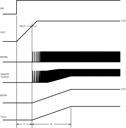 Figure 1. Start-Up Sequence
6.8 Typical Characteristics
at TA = 25°C (unless otherwise noted)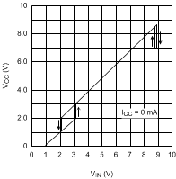 Figure 2. VCC vs VIN
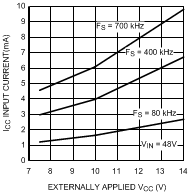 Figure 4. ICC vs Externally Applied VCC
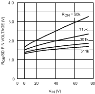 Figure 6. Voltage at RON/SD Pin
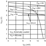 Figure 3. VCC vs ICC
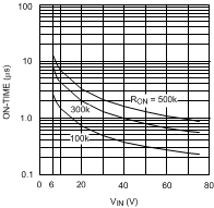 Figure 5. ON-Time vs VIN and RON
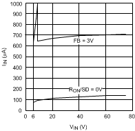 Figure 7. IIN vs VIN