-
LM5012-Q1 Automotive 100-V Input, 2.5-A Non-Synchronous Buck DC/DC Converter With Ultra-low IQ
- 1 Features
- 2 Applications
- 3 Description
- 4 Revision History
- 5 Device Comparison Table
- 6 Pin Configuration and Functions
- 7 Specifications
-
8 Detailed Description
- 8.1 Overview
- 8.2 Functional Block Diagram
- 8.3
Feature Description
- 8.3.1 Control Architecture
- 8.3.2 Internal VCC Regulator and Bootstrap Capacitor
- 8.3.3 Regulation Comparator
- 8.3.4 Internal Soft Start
- 8.3.5 On-Time Generator
- 8.3.6 Current Limit
- 8.3.7 N-Channel Buck Switch and Driver
- 8.3.8 Schottky Diode Selection
- 8.3.9 Enable/Undervoltage Lockout (EN/UVLO)
- 8.3.10 Power Good (PGOOD)
- 8.3.11 Thermal Protection
- 8.4 Device Functional Modes
- 9 Application and Implementation
- 10Device and Documentation Support
- 11Mechanical, Packaging, and Orderable Information
- IMPORTANT NOTICE
Package Options
Mechanical Data (Package|Pins)
- DDA|8
Thermal pad, mechanical data (Package|Pins)
- DDA|8
Orderable Information
LM5012-Q1 Automotive 100-V Input, 2.5-A Non-Synchronous Buck DC/DC Converter With Ultra-low IQ
1 Features
- AEC-Q100-qualified for automotive
applications
- Device temperature grade 1: –40°C to +125°C, ambient temperature range
- Functional Safety-Capable
- Designed for reliable and rugged
applications
- Wide input voltage range of 6 V to 100 V
- –40°C to +150°C junction temperature range
- Fixed 3.5-ms internal soft-start timer
- Peak current-limit protection
- Input UVLO and thermal shutdown protection
- Optimized for ultra-low EMI
requirements
- Meets CISPR 25 Class 5 standard
- Suited for scalable automotive
power supplies
- Pin-to-pin compatible with the LM5163-Q1 LM5164-Q1 (100 V, 0.5 A or 1 A), and LM5013-Q1 (100 V, 3.5 A)
- 50-ns low minimum on times and off times
- 10-µA no-load sleep current
- 3.1-µA shutdown quiescent current
- Integration reduces solution size
and cost
- COT mode control architecture
- Integrated 100-V, 0.25-Ω power MOSFET
- 1.2-V internal voltage reference
- No loop compensation components
- Internal VCC bias regulator and boot diode
- Create a custom regulator design with the LM5013-Q1 using WEBENCH® Power Designer
3 Description
With an integrated high-side power MOSFET, the LM5012-Q1 delivers up to 2.5 A of output current. A constant on-time (COT) control architecture provides nearly constant switching frequency with excellent load and line transient response. Additional features of the LM5012-Q1 include ultra-low IQ operation for high light-load efficiency, innovative peak overcurrent protection, integrated VCC bias supply and bootstrap diode, precision enable and input UVLO, and thermal shutdown protection with automatic recovery. An open-drain PGOOD indicator provides sequencing, fault reporting, and output voltage monitoring.
The LM5012-Q12.5 A is qualified to automotive AEC-Q100 grade 1 and is available in a 8-pin SO PowerPAD™ integrated circuit package. The device 1.27-mm pin pitch provides adequate spacing for high-voltage applications.
| Part Number | Package(1) | Body Size (NOM) |
|---|---|---|
| LM5012-Q1 | DDA (SO PowerPAD, 8) | 4.89 mm × 3.90 mm |
 Typical Application
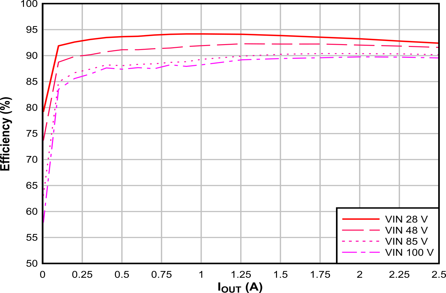
Efficiency, VOUT = 12 V