-
LM5066 10 to 80 V, Hotswap Controller With I/V/P Monitoring and PMBus Interface
- 1 Features
- 2 Applications
- 3 Description
- 4 Revision History
- 5 Device Comparison Table
- 6 Pin Configuration and Functions
- 7 Specifications
-
8 Detailed Description
- 8.1 Overview
- 8.2 Functional Block Diagram
- 8.3 Feature Description
- 8.4 Device Functional Modes
- 8.5
Programming
- 8.5.1 PMBus Command Support
- 8.5.2
Standard PMBus Commands
- 8.5.2.1 OPERATION (01h)
- 8.5.2.2 CLEAR_FAULTS (03h)
- 8.5.2.3 CAPABILITY (19h)
- 8.5.2.4 VOUT_UV_WARN_LIMIT (43h)
- 8.5.2.5 OT_FAULT_LIMIT (4Fh)
- 8.5.2.6 OT_WARN_LIMIT (51h)
- 8.5.2.7 VIN_OV_WARN_LIMIT (57h)
- 8.5.2.8 VIN_UV_WARN_LIMIT (58h)
- 8.5.2.9 STATUS_BYTE (78h)
- 8.5.2.10 STATUS_WORD (79h)
- 8.5.2.11 STATUS_VOUT (7Ah)
- 8.5.2.12 STATUS_INPUT (7Ch)
- 8.5.2.13 STATUS_TEMPERATURE (7dh)
- 8.5.2.14 STATUS_CML (7Eh)
- 8.5.2.15 STATUS_MFR_SPECIFIC (80h)
- 8.5.2.16 READ_VIN (88h)
- 8.5.2.17 READ_VOUT (8Bh)
- 8.5.2.18 READ_TEMPERATURE_1 (8Dh)
- 8.5.2.19 MFR_ID (99h)
- 8.5.2.20 MFR_MODEL (9Ah)
- 8.5.2.21 MFR_REVISION (9Bh)
- 8.5.3
Manufacturer Specific PMBus Commands
- 8.5.3.1 MFR_SPECIFIC_00: READ_VAUX (D0h)
- 8.5.3.2 MFR_SPECIFIC_01: MFR_READ_IIN (D1h)
- 8.5.3.3 MFR_SPECIFIC_02: MFR_READ_PIN (D2h)
- 8.5.3.4 MFR_SPECIFIC_03: MFR_IN_OC_WARN_LIMIT (D3h)
- 8.5.3.5 MFR_SPECIFIC_04: MFR_PIN_OP_WARN_LIMIT (D4h)
- 8.5.3.6 MFR_SPECIFIC_05: READ_PIN_PEAK (D5h)
- 8.5.3.7 MFR_SPECIFIC_06: CLEAR_PIN_PEAK (D6h)
- 8.5.3.8 MFR_SPECIFIC_07: GATE_MASK (D7h)
- 8.5.3.9 MFR_SPECIFIC_08: ALERT_MASK (D8h)
- 8.5.3.10 MFR_SPECIFIC_09: DEVICE_SETUP (D9h)
- 8.5.3.11 MFR_SPECIFIC_10: BLOCK_READ (DAh)
- 8.5.3.12 MFR_SPECIFIC_11: SAMPLES_FOR_AVG (DBh)
- 8.5.3.13 MFR_SPECIFIC_12: READ_AVG_VIN (DCh)
- 8.5.3.14 MFR_SPECIFIC_13: READ_AVG_VOUT (DDh)
- 8.5.3.15 MFR_SPECIFIC_14: READ_AVG_IIN (DEh)
- 8.5.3.16 MFR_SPECIFIC_15: READ_AVG_PIN
- 8.5.3.17 MFR_SPECIFIC_16: BLACK_BOX_READ (E0h)
- 8.5.3.18 MFR_SPECIFIC_17: READ_DIAGNOSTIC_WORD (E1h)
- 8.5.3.19 MFR_SPECIFIC_18: AVG_BLOCK_READ (E2h)
- 8.5.4 Reading and Writing Telemetry Data and Warning Thresholds
- 8.5.5 Determining Telemetry Coefficients Empirically With Linear Fit
- 8.5.6 Writing Telemetry Data
- 8.5.7 PMBus Address Lines (ADR0, ADR1, ADR2)
- 8.5.8 SMBA Response
-
9 Application and Implementation
- 9.1 Application Information
- 9.2
Typical Application
- 9.2.1
48-V, 10-A PMBus Hotswap Design
- 9.2.1.1 Design Requirements
- 9.2.1.2
Detailed Design-In Procedure
- 9.2.1.2.1 Select RSNS and CL Setting
- 9.2.1.2.2 Selecting the Hotswap FETs
- 9.2.1.2.3 Select Power Limit
- 9.2.1.2.4 Set Fault Timer
- 9.2.1.2.5 Check MOSFET SOA
- 9.2.1.2.6 Set UVLO and OVLO Thresholds
- 9.2.1.2.7 Power Good Pin
- 9.2.1.2.8 Input and Output Protection
- 9.2.1.2.9 Final Schematic and Component Values
- 9.2.1.3 Application Curves
- 9.2.1
48-V, 10-A PMBus Hotswap Design
- 10Power Supply Recommendations
- 11Layout
- 12Device and Documentation Support
- 13Mechanical, Packaging, and Orderable Information
- IMPORTANT NOTICE
Package Options
Mechanical Data (Package|Pins)
- PWP|28
Thermal pad, mechanical data (Package|Pins)
- PWP|28
Orderable Information
LM5066 10 to 80 V, Hotswap Controller With I/V/P Monitoring and PMBus Interface
1 Features
- 10- to 80-V Operation
- 100-V Continuous Absolute Max
- 26 mV (±12%) or 50 mV (±6%) ILIM Threshold
- Programmable FET SOA Protection
- Programable UV, OV, tFAULT Thresholds
- External FET Temperature Sensing
- Failed FET Detection
- I2C / SMBus Interface
- PMBus™ Compliant Command Structure
- Precision V IN, VOUT, IIN, PIN, VAUX Monitoring
- V (±2.7%); I (±3%); P (±4.5%)
- Programable I/V/P Averaging Interval
- 12-bit ADC with 1-kHz Sampling Rate
- –40°C < TJ < 125°C Operation
- Pin-to-Pin Compatible with LM5066I
2 Applications
- 48-V Servers
- Base Station Power Distribution
- Networking Routers and Switchers
- PLC Power Management
- 24- to 28-V Industrial Systems
3 Description
LM5066 provides robust protection and precision monitoring for 10- to 80-V systems. Programmable UV, OV, ILIMIT, and fast-short circuit protection allow for customized protection for any application. Programmable FET SOA protection sets the maximum power the FET is allowed to dissipate under any condition. The programmable fault timer (tFAULT) is set to avoid nuisance trips, ensure start-up, and limit the duration of over load events.
In addition to circuit protection, the LM5066 supplies real-time power, voltage, current, temperature, and fault data to the system management host through the I2C / SMBus interface. PMBus compliant command structure makes it easy to program the device. Precision telemetry enables intelligent power management functions such as efficiency optimization and early fault detection. LM5066 also supports advanced features such as I/V/P averaging and peak power measurment to improve system diagnostics.
LM5066I is pin-to-pin compatible with the LM5066 and offers improved telemetry accuracy and supports the Read_Ein command to monitor energy. See Table 1 for a detailed comparison.
Device Information(1)
| PART NUMBER | PACKAGE | BODY SIZE (NOM) |
|---|---|---|
| LM5066 | PWP (28) | 9.70 × 4.40 mm2 |
SPACE
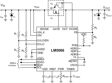
Simplified Schematic

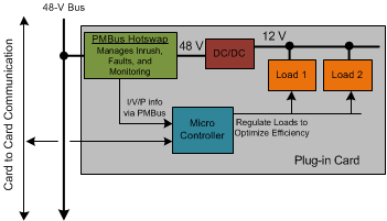
LM5066 in a Plug-in Card

4 Revision History
Changes from H Revision (July 2014) to I Revision
- Changed VGATEZ MIN value in Electrical Characteristics From: 15 V To: 12 V Go
Changes from G Revision (February 2013) to H Revision
- Updated data sheet to new TI standards: added new sections and reordered document flow Go
- Added link to LM5066 design calculator Go
Changes from F Revision (February 2013) to G Revision
- Changed layout of National Data Sheet to TI formatGo
Changes from A Revision (May 2014) to B Revision
- Changed title of Handling Ratings table to ESD Ratings table Go
5 Device Comparison Table
Table 1 summarizes the differences between the LM5066 and the LM5066I. Note that the current monitoring accuracy of the LM5066I is much better at the ILIM = 26 mV setting, but is comparable at the 50-mV setting. For many applications with lower power, using the LM5066 at the 50-mV setting is a great option. However, for higher power applications upgrading to LM5066I and using the ILIM = 26 mV setting will lead to significant power savings (approximately 24 mV × ILOAD). In addition, the higher accuracy and energy monitoring capability can enable further improvements in system efficiency, which is critical in high power applications.
Table 1. LM5066 vs LM5066I
| KEY PARAMETERS | LM5066 | LM5066I |
|---|---|---|
| Voltage monitoring | ±2.7% | ±1.25% |
| Current monitoring (ILIM = 26 mV) | ±4.25% | ±1.75% |
| Power monitoring (ILIM = 26 mV) | ±4.5% | ±.2.5% |
| Current monitoring (ILIM = 50 mV) | ±3% | ±3.5% |
| Power monitoring (ILIM = 50 mV) | ±4.5% | ±4.5% |
| Supports Energy Monitoring via Read_EIN command | No | Yes |