-
LM5109B-Q1 High Voltage 1-A Peak Half Bridge Gate Driver
- 1 Features
- 2 Applications
- 3 Description
- 4 Revision History
- 5 Detailed Description
- 6 Application and Implementation
- 7 Power Supply Recommendations
- 8 Layout
- 9 Device and Documentation Support
- 10Mechanical, Packaging, and Orderable Information
- IMPORTANT NOTICE
Package Options
Mechanical Data (Package|Pins)
- NGT|8
Thermal pad, mechanical data (Package|Pins)
Orderable Information
LM5109B-Q1 High Voltage 1-A Peak Half Bridge Gate Driver
1 Features
- Qualified for Automotive Applications
- AEC-Q100 Qualified With the Following Results
- Device Temperature Grade 1
- Device HBM ESD Classification Level 1C
- Device CDM ESD Classification Level C4A
- Drives Both a High-Side and Low-Side N-Channel MOSFET
- 1-A Peak Output Current (1.0-A Sink/1.0-A Source)
- Independent TTL/CMOS Compatible Inputs
- Bootstrap Supply Voltage to 108-V DC
- Fast Propagation Times (30 ns Typical)
- Drives 1000-pF Load with 15-ns Rise and Fall Times
- Excellent Propagation Delay Matching (2 ns Typical)
- Supply Rail Under-Voltage Lockout
- Low Power Consumption
- Thermally-Enhanced WSON-8 Package
2 Applications
- Push-Pull Converters
- Half and Full Bridge Power Converters
- Solid State Motor Drives
- Two Switch Forward Power Converters
3 Description
The LM5109B-Q1 is a cost effective, high voltage gate driver designed to drive both the high-side and the low-side N-Channel MOSFETs in a synchronous buck or a half bridge configuration. The floating high-side driver is capable of working with rail voltages up to 90 V. The outputs are independently controlled with TTL/CMOS compatible logic input thresholds. The robust level shift technology operates at high speed while consuming low power and providing clean level transitions from the control input logic to the high-side gate driver. Under-voltage lockout is provided on both the low-side and the high-side power rails. The device is available in the thermally enhanced WSON(8) packages.
Device Information(1)
| PART NUMBER | PACKAGE | BODY SIZE (NOM) |
|---|---|---|
| LM5109B-Q1 | WSON (8) | 4.00 mm × 4.00 mm |
- For all available packages, see the orderable addendum at the end of the data sheet.
Simplified Application Diagram

4 Revision History
Changes from * Revision (November 2015) to A Revision
- Changed device from Product Preview to Production Data and released full data sheetGo
Specifications
4.1 Absolute Maximum Ratings
over operating free-air temperature range (unless otherwise noted)(1)| MIN | MAX | UNIT | |
|---|---|---|---|
| VDD to VSS | –0.3 | 18 | V |
| HB to HS | –0.3 | 18 | V |
| LI or HI to VSS | –0.3 | VDD + 0.3 | V |
| LO to VSS | –0.3 | VDD + 0.3 | V |
| HO to VSS | VHS – 0.3 | VHB + 0.3 | V |
| HS to VSS(1) | –5 | 90 | V |
| HB to VSS | 108 | V | |
| Junction temperature | –40 | 150 | °C |
| Storage temperature, Tstg | –55 | 150 | °C |
4.2 ESD Ratings
| VALUE | UNIT | |||
|---|---|---|---|---|
| V(ESD) | Electrostatic discharge | Human-body model (HBM), per AEC Q100-002(1) | 1500 | V |
| Charged-device model (CDM), per AEC Q100-011 | 750 | |||
4.3 Recommended Operating Conditions
over operating free-air temperature range (unless otherwise noted)| MIN | NOM | MAX | UNIT | ||
|---|---|---|---|---|---|
| VDD | 8 | 14 | V | ||
| HS(1) | –1 | 90 | V | ||
| HB | VHS+8 | VHS+14 | V | ||
| HS Slew Rate | < 50 | V/ns | |||
| Junction Temperature | –40 | 125 | °C | ||
4.4 Thermal Information
| THERMAL METRIC(1) | LM5109B-Q1 | UNIT | |
|---|---|---|---|
| NGT (WSON) | |||
| 8-PINS | |||
| RθJA | Junction-to-ambient thermal resistance | 42.3 | °C/W |
| RθJC(top) | Junction-to-case (top) thermal resistance | 34.0 | °C/W |
| RθJB | Junction-to-board thermal resistance | 19.3 | °C/W |
| ψJT | Junction-to-top characterization parameter | 0.4 | °C/W |
| ψJB | Junction-to-board characterization parameter | 19.5 | °C/W |
| RθJC(bot) | Junction-to-case (bottom) thermal resistance | 8.1 | °C/W |
4.5 Electrical Characteristics
TJ = 25°C (unless otherwise noted)VDD = VHB = 12 V, VSS = VHS = 0 V, No Load on LO or HO.
| PARAMETER | TEST CONDITIONS | MIN | TYP | MAX | UNIT | ||
|---|---|---|---|---|---|---|---|
| Supply Currents | |||||||
| IDD | VDD Quiescent Current | LI = HI = 0V | TJ = 25°C | 0.3 | mA | ||
| TJ = –40°C to 125°C | 0.6 | ||||||
| IDDO | VDD Operating Current | f = 500 kHz | TJ = 25°C | 1.8 | mA | ||
| TJ = –40°C to 125°C | 2.9 | ||||||
| IHB | Total HB Quiescent Current | LI = HI = 0V | TJ = 25°C | 0.06 | mA | ||
| TJ = –40°C to 125°C | 0.2 | ||||||
| IHBO | Total HB Operating Current | f = 500 kHz | TJ = 25°C | 1.4 | mA | ||
| TJ = –40°C to 125°C | 2.8 | ||||||
| IHBS | HB to VSS Current, Quiescent | VHS = VHB = 90V | TJ = 25°C | 0.1 | µA | ||
| TJ = –40°C to 125°C | 10 | ||||||
| IHBSO | HB to VSS Current, Operating | f = 500 kHz | 0.5 | mA | |||
| Input Pins Li and Hi | |||||||
| VIL | Low Level Input Voltage Threshold | TJ = 25°C | 1.8 | V | |||
| TJ = –40°C to 125°C | 0.8 | ||||||
| VIH | High Level Input Voltage Threshold | TJ = 25°C | 1.8 | V | |||
| TJ = –40°C to 125°C | 2.2 | ||||||
| RI | Input Pulldown Resistance | TJ = 25°C | 200 | kΩ | |||
| TJ = –40°C to 125°C | 100 | 500 | |||||
| Under Voltage Protection | |||||||
| VDDR | VDD Rising Threshold | VDDR = VDD - VSS | TJ = 25°C | 6.7 | V | ||
| TJ = –40°C to 125°C | 6.0 | 7.4 | |||||
| VDDH | VDD Threshold Hysteresis | 0.5 | V | ||||
| VHBR | HB Rising Threshold | VHBR = VHB - VHS | TJ = 25°C | 6.6 | V | ||
| TJ = –40°C to 125°C | 5.7 | 7.1 | |||||
| VHBH | HB Threshold Hysteresis | 0.4 | V | ||||
| LO Gate Driver | |||||||
| VOLL | Low-Level Output Voltage | ILO = 100 mA, VOHL = VLO – VSS | TJ = 25°C | 0.38 | V | ||
| TJ = –40°C to 125°C | 0.65 | ||||||
| VOHL | High-Level Output Voltage | ILO = −100 mA, VOHL = VDD– VLO | TJ = 25°C | 0.72 | V | ||
| TJ = –40°C to 125°C | 1.20 | ||||||
| IOHL | Peak Pullup Current | VLO = 0V | 1.0 | A | |||
| IOLL | Peak Pulldown Current | VLO = 12V | 1.0 | A | |||
| HO Gate Driver | |||||||
| VOLH | Low-Level Output Voltage | IHO = 100 mA, VOLH = VHO– VHS | TJ = 25°C | 0.38 | V | ||
| TJ = –40°C to 125°C | 0.65 | ||||||
| VOHH | High-Level Output Voltage | IHO = −100 mA, VOHH = VHB– VHO | TJ = 25°C | 0.72 | V | ||
| TJ = –40°C to 125°C | 1.20 | ||||||
| IOHH | Peak Pullup Current | VHO = 0V | 1.0 | A | |||
| IOLH | Peak Pulldown Current | VHO = 12V | 1.0 | A | |||
4.6 Switching Characteristics
TJ = 25°C (unless otherwise noted)VDD = VHB = 12 V, VSS = VHS = 0 V, No Load on LO or HO.
| PARAMETER | TEST CONDITIONS | MIN | TYP | MAX | UNIT | |
|---|---|---|---|---|---|---|
| tLPHL | Lower Turn-Off Propagation Delay (LI Falling to LO Falling) |
TJ = 25°C | 30 | ns | ||
| TJ = –40°C to 125°C | 56 | |||||
| tHPHL | Upper Turn-Off Propagation Delay (HI Falling to HO Falling) |
TJ = 25°C | 30 | ns | ||
| TJ = –40°C to 125°C | 56 | |||||
| tLPLH | Lower Turn-On Propagation Delay (LI Rising to LO Rising) |
TJ = 25°C | 32 | ns | ||
| TJ = –40°C to 125°C | 56 | |||||
| tHPLH | Upper Turn-On Propagation Delay (HI Rising to HO Rising) |
TJ = 25°C | 32 | ns | ||
| TJ = –40°C to 125°C | 56 | |||||
| tMON | Delay Matching: Lower Turn-On and Upper Turn-Off | TJ = 25°C | 2 | ns | ||
| TJ = –40°C to 125°C | 15 | |||||
| tMOFF | Delay Matching: Lower Turn-Off and Upper Turn-On | TJ = 25°C | 2 | ns | ||
| TJ = –40°C to 125°C | 15 | |||||
| tRC, tFC | Either Output Rise/Fall Time | CL = 1000 pF | 15 | ns | ||
| tPW | Minimum Input Pulse Width that Changes the Output | 50 | ns | |||
4.7 Typical Characteristics
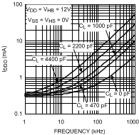
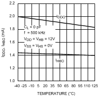
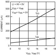
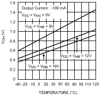 Figure 8. LO and HO High Level Output Voltage vs Temperature
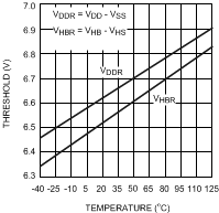 Figure 10. Undervoltage Rising Thresholds vs Temperature
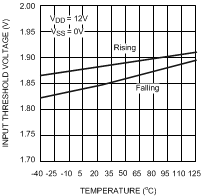 Figure 12. Input Thresholds vs Temperature
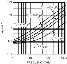
| VDD = VHB = 12 V | VSS = VHS = 0 V |
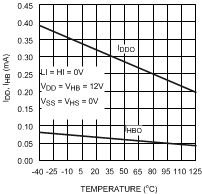
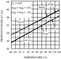
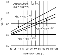 Figure 9. LO and HO Low Level Output Voltage vs Temperature
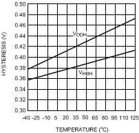 Figure 11. Undervoltage Hysteresis vs Temperature
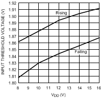 Figure 13. Input Thresholds vs Supply Voltage
5 Detailed Description
5.1 Overview
The LM5109B-Q1 is a cost-effective, high voltage gate driver designed to drive both the high-side and the low-side N-channel FETs in a synchronous buck or a half-bridge configuration. The outputs are independently controlled with TTL/CMOS compatible input thresholds. The floating high-side driver is capable of working with HB voltage up to 108 V. An external high voltage diode must be provided to charge high side gate drive bootstrap capacitor. A robust level shifter operates at high speed while consuming low power and providing clean level transitions from the control logic to the high side gate driver. Under-voltage lockout (UVLO) is provided on both the low side and the high side power rails.
5.2 Functional Block Diagram
5.3 Feature Description
5.3.1 Start-up and UVLO
Both top and bottom drivers include UVLO protection circuitry which monitors the supply voltage (VDD) and bootstrap capacitor voltage (VHB–HS) independently. The UVLO circuit inhibits each output until sufficient supply voltage is available to turn on the external MOSFETs, and the built-in UVLO hysteresis prevents chattering during supply voltage variations. When the supply voltage is applied to the VDD pin of the LM5109B-Q1, the top and bottom gates are held low until VDD exceeds the UVLO threshold, typically about 6.7 V. Any UVLO condition on the bootstrap capacitor (VHB–HS) will only disable the high- side output (HO).
Table 1. VDD UVLO Feature Logic Operation
| Condition (VHB-HS>VHBR for all case below) | HI | LI | HO | LO |
|---|---|---|---|---|
| VDD-VSS < VDDR during device start-up | H | L | L | L |
| VDD-VSS < VDDR during device start-up | L | H | L | L |
| VDD-VSS < VDDR during device start-up | H | H | L | L |
| VDD-VSS < VDDR during device start-up | L | L | L | L |
| VDD-VSS < VDDR – VDDH after device start-up | H | L | L | L |
| VDD-VSS < VDDR – VDDH after device start-up | L | H | L | L |
| VDD-VSS < VDDR – VDDH after device start-up | H | H | L | L |
| VDD-VSS < VDDR – VDDH after device start-up | L | L | L | L |
Table 2. VHB-HS UVLO Feature Logic Operation
| Condition (VDD>VDDR for all case below) | HI | LI | HO | LO |
|---|---|---|---|---|
| VHB-HS < VHBR during device start-up | H | L | L | L |
| VHB-HS < VHBR during device start-up | L | H | L | H |
| VHB-HS < VHBR during device start-up | H | H | L | H |
| VHB-HS < VHBR during device start-up | L | L | L | L |
| VHB-HS < VHBR – VHBH after device start-up | H | L | L | L |
| VHB-HS < VHBR – VHBH after device start-up | L | H | L | H |
| VHB-HS < VHBR – VHBH after device start-up | H | H | L | H |
| VHB-HS < VHBR – VHBH after device start-up | L | L | L | L |
5.3.2 Level Shift
The level shift circuit is the interface from the high-side input to the high-side driver stage which is referenced to the switch node (HS). The level shift allows control of the HO output which is referenced to the HS pin and provides excellent delay matching with the low-side driver.
5.3.3 Output Stages
The output stages are the interface to the power MOSFETs in the power train. High slew rate, low resistance, and high peak current capability of both outputs allow for efficient switching of the power MOSFETs. The low-side output stage is referenced to VSS and the high-side is referenced to HS.
5.4 HS Transient Voltages Below Ground
The HS node will always be clamped by the body diode of the lower external FET. In some situations, board resistances and inductances can cause the HS node to transiently swing several volts below ground. The HS node can swing below ground provided:
- HS must always be at a lower potential than HO. Pulling HO more than –0.3 V below HS can activate parasitic transistors resulting in excessive current flow from the HB supply, possibly resulting in damage to the IC. The same relationship is true with LO and VSS. If necessary, a Schottky diode can be placed externally between HO and HS or LO and GND to protect the IC from this type of transient. The diode must be placed as close to the IC pins as possible in order to be effective.
- HB to HS operating voltage should be 15 V or less. Hence, if the HS pin transient voltage is –5 V, VDD should be ideally limited to 10 V to keep HB to HS below 15 V.
- Low ESR bypass capacitors from HB to HS and from VDD to VSS are essential for proper operation. The capacitor should be located at the leads of the IC to minimize series inductance. The peak currents from LO and HO can be quite large. Any series inductances with the bypass capacitor will cause voltage ringing at the leads of the IC which must be avoided for reliable operation.
5.5 Device Functional Modes
The device operates in normal mode and UVLO mode. See Start-up and UVLO for more information on UVLO operation mode. In normal mode when the VDD and VHB–HS are above UVLO threshold, the output stage is dependent on the states of the HI and LI pins. The output HO and LO will be low if input state is floating.