LM75A Digital Temperature Sensor and Thermal Watchdog With Two-Wire Interface
1 Features
- No External Components Required
- Shutdown Mode to Minimize Power Consumption
- Up to Eight LM75As can be Connected to a Single Bus
- Power up Defaults Permit Stand-Alone Operation as Thermostat
- Key Specifications:
- Supply Voltage
- LM75A: 2.7 V to 5.5 V
- Supply Current
- Operating: 280 μA (Typical)
- Shutdown: 4 μA (Typical)
- Temperature Accuracy
- 25°C to 100°C: ±2°C (Max)
- 55°C to 125°C: ±3°C (Max)
- Supply Voltage
2 Applications
- General System Thermal Management
- Communications Infrastructure
- Electronic Test Equipment
- Environmental Monitoring
3 Description
The LM75A is an industry-standard digital temperature sensor with an integrated sigma-delta analog-to-digital converter (ADC) and I2C interface. The LM75A provides 9-bit digital temperature readings with an accuracy of ±2°C from –25°C to 100°C and ±3°C over –55°C to 125°C.
The LM75A operates with a single supply from 2.7 V to 5.5 V. Communication is accomplished over a
2-wire interface which operates up to 400 kHz. The LM75A has three address pins, allowing up to eight LM75A devices to operate on the same 2-wire bus. The LM75A has a dedicated overtemperature output (O.S.) with programmable limit and hysteresis. This output has programmable fault tolerance, which lets the user to define the number of consecutive error conditions that must occur before O.S. is activated. The wide temperature and supply range and I2C interface make the LM75A ideal for a number of applications including base stations, electronic test equipment, office electronics, personal computers, and any other system in which thermal management is critical to performance. The LM75A is available in an SOIC-8 package and an VSSOP-8 package.
Device Information(1)
| PART NUMBER | PACKAGE | BODY SIZE (NOM) |
|---|---|---|
| LM75A | SOIC (8) | 4.90 mm × 3.91 mm |
| VSSOP (8) | 3.00 mm × 3.00 mm |
- For all available packages, see the orderable addendum at the end of the datasheet.
Typical Application

4 Revision History
Changes from O Revision (May 2013) to P Revision
- Added Pin Configuration and Functions section, ESD Ratings table, Feature Description section, Device Functional Modes, Application and Implementation section, Power Supply Recommendations section, Layout section, Device and Documentation Support section, and Mechanical, Packaging, and Orderable Information section Go
Changes from N Revision (May 2013) to O Revision
- Changed layout of National Data Sheet to TI formatGo
5 Pin Configuration and Functions

Pin Functions
| PIN | DESCRIPTION | TYPICAL CONNECTION | |
|---|---|---|---|
| NO. | NAME | ||
| 1 | SDA | I2C Serial Bi-Directional Data Line, Open Drain | From Controller, tied to a pullup resistor or current source |
| 2 | SCL | I2C Clock Input | From Controller, tied to a pullup resistor or current source |
| 3 | O.S. | Overtemperature Shutdown, Open Drain Output | Pull–up Resistor, Controller Interrupt Line |
| 4 | GND | Power Supply Ground | Ground |
| 5 | A2 | User-Set I2C Address Inputs | Ground (Low, “0”) or +VS (High, “1”) |
| 6 | A1 | ||
| 7 | A0 | ||
| 8 | +VS | Positive Supply Voltage Input | DC Voltage from 2.7 V to 5.5 V 100-nF bypass capacitor with 10-µF bulk capacitance in the near vicinity |
6 Specifications
6.1 Absolute Maximum Ratings
over operating free-air temperature range (unless otherwise noted)(1)| MIN | MAX | UNIT | |||
|---|---|---|---|---|---|
| Supply Voltage Pin (+VS) | −0.3 | 6.5 | V | ||
| Voltage at A0, A1and A2 Pins | −0.3 | (+VS + 0.3) and must be ≤ 6.5 | V | ||
| Voltage at OS, SCL and SDA Pins | −0.3 | 6.5 | V | ||
| Input Current at any Pin(2) | 5 | mA | |||
| Package Input Current(2) | 20 | mA | |||
| O.S. Output Sink Current | 10 | mA | |||
| O.S. Output Voltage | 6.5 | V | |||
| Storage temperature, Tstg | –65 | 150 | °C | ||
6.2 ESD Ratings
| VALUE | UNIT | |||
|---|---|---|---|---|
| V(ESD) | Electrostatic discharge | Human-body model (HBM), per ANSI/ESDA/JEDEC JS-001(1) | ±2500 | V |
| Charged-device model (CDM), per JEDEC specification JESD22-C101(2) | ±1000 | |||
| Machine model | ±250 | |||
6.3 Recommended Operating Conditions(4)(3)
| MIN | MAX | UNIT | |
|---|---|---|---|
| Specified Temperature Range (TMIN to TMAX) | −55 | 125 | °C |
| Supply Voltage Range (+VS) LM75A | 2.7 | 5.5 | V |
6.4 Thermal Information
| THERMAL METRIC(1) | LM75A | UNIT | ||
|---|---|---|---|---|
| D | DGK | |||
| 8 PINS | 8 PINS | |||
| RθJA | Junction-to-ambient thermal resistance | 200 | 250 | °C/W |
6.5 Temperature-to-Digital Converter Characteristics
Unless otherwise noted, these specifications apply for: +VS = 2.7 to 5.5 Vdc for LM75AIM. TA = TJ = 25°C, unless otherwise noted.| PARAMETER | TEST CONDITIONS | MIN | TYP(9) | MAX(5) | UNIT | ||
|---|---|---|---|---|---|---|---|
| Accuracy | TA = −25°C to +100°C –55°C ≤ TJ ≤ 125°C |
–2 | 2 | °C | |||
| TA = −55°C to +125°C –55°C ≤ TJ ≤ 125°C |
–3 | 3 | |||||
| Resolution | 9 | Bits | |||||
| Temperature Conversion Time | See(6) | 100 | ms | ||||
| See(6), –55°C ≤ TJ ≤ 125°C | 300 | ||||||
| Quiescent Current | LM75A | I2C Inactive | 0.28 | mA | |||
| I2C Inactive, –55°C ≤ TJ ≤ 125°C | 0.5 | ||||||
| Shutdown Mode, +VS = 3 V | 4 | μA | |||||
| Shutdown Mode, +VS = 5 V | 6 | μA | |||||
| O.S. Output Saturation Voltage | IOUT = 4 mA, –55°C ≤ TJ ≤ 125°C | 0.8 | V | ||||
| O.S. Delay | See(7), –55°C ≤ TJ ≤ 125°C | 1 | 6 | Conversion | |||
| TOS Default Temperature | See(8) | 80 | °C | ||||
| THYST Default Temperature | See(8) | 75 | °C | ||||
6.6 Digital DC Characteristics
Unless otherwise noted, these specifications apply for +VS = 2.7 to 5.5 Vdc for LM75AIM and LM75AIMM. TA = TJ = 25°C, unless otherwise noted.| PARAMETER | TEST CONDITIONS | MIN | TYP(9) | MAX(5) | UNIT | ||
|---|---|---|---|---|---|---|---|
| VIN(1) | Logical “1” Input Voltage | –55°C ≤ TJ ≤ 125°C | +VS × 0.7 | +VS + 0.3 | V | ||
| V | |||||||
| VIN(0) | Logical “0” Input Voltage | –55°C ≤ TJ ≤ 125°C | −0.3 | +VS × 0.3 | V | ||
| V | |||||||
| IIN(1) | Logical “1” Input Current | VIN = +VS | 0.005 | μA | |||
| VIN = +VS, –55°C ≤ TJ ≤ 125°C | 1.0 | ||||||
| IIN(0) | Logical “0” Input Current | VIN = 0 V | −0.005 | μA | |||
| VIN = 0 V, –55°C ≤ TJ ≤ 125°C | −1.0 | ||||||
| CIN | All Digital Inputs | 5 | pF | ||||
| IOH | High Level Output Current Open drain leakage |
LM75A | VOH = 5 V, –55°C ≤ TJ ≤ 125°C | 1 | μA | ||
| VOL | Low Level Output Voltage | IOL = 3 mA, –55°C ≤ TJ ≤ 125°C | 0.4 | V | |||
| tOF | Output Fall Time | CL = 400 pF IO = 3 mA, –55°C ≤ TJ ≤ 125°C | 250 | ns | |||
6.7 I2C Digital Switching Characteristics
Unless otherwise noted, these specifications apply for +VS = 2.7 to 5.5 Vdc for LM75AIM and LM75AIMM on output lines = 80 pF unless otherwise specified. TA = TJ = 25°C, unless otherwise noted.| PARAMETER | TEST CONDITIONS | MIN | TYP(9) | MAX(5)(11) | UNIT | ||
|---|---|---|---|---|---|---|---|
| t1 | SCL (Clock) Period | –55°C ≤ TJ ≤ 125°C | 2.5 | ns | |||
| t2 | Data in Set-Up Time to SCL High | –55°C ≤ TJ ≤ 125°C | 100 | ns | |||
| t3 | Data Out Stable after SCL Low | –55°C ≤ TJ ≤ 125°C | 0 | ns | |||
| t4 | SDA Low Set-Up Time to SCL Low (Start Condition) | –55°C ≤ TJ ≤ 125°C | 100 | ns | |||
| t5 | SDA High Hold Time after SCL High (Stop Condition) | –55°C ≤ TJ ≤ 125°C | 100 | ns | |||
| tTIMEOUT | SDA Time Low for Reset of Serial Interface(10) | LM75A | 75 | ms | |||
| –55°C ≤ TJ ≤ 125°C | 325 | ||||||
 Figure 1. Timing Diagram
 Figure 2. Temperature-to-Digital Transfer Function (Non-Linear Scale for Clarity)
 Figure 3. Printed Circuit Board Used for Thermal Resistance Specifications
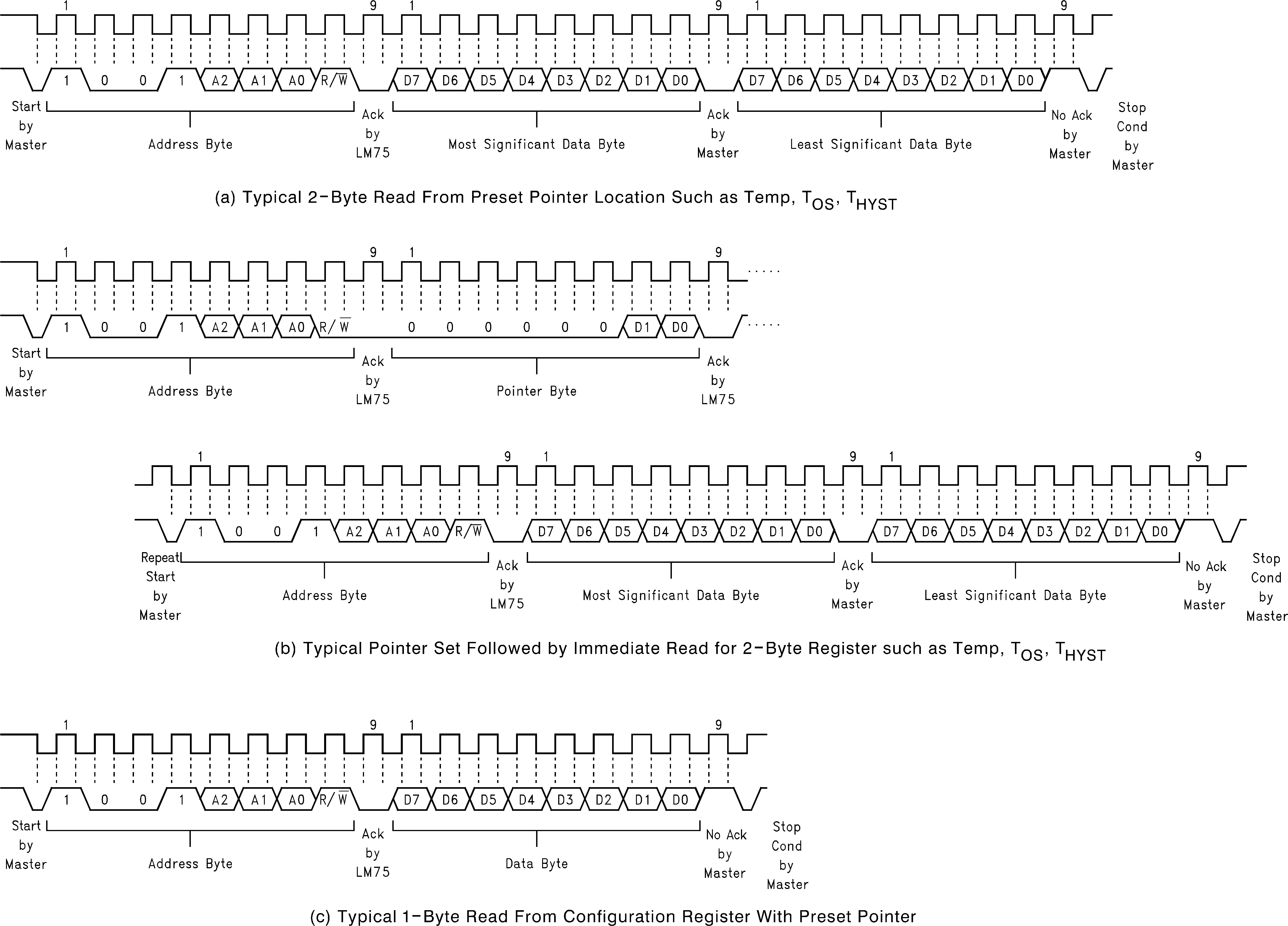 Figure 4. I2C Timing Diagram
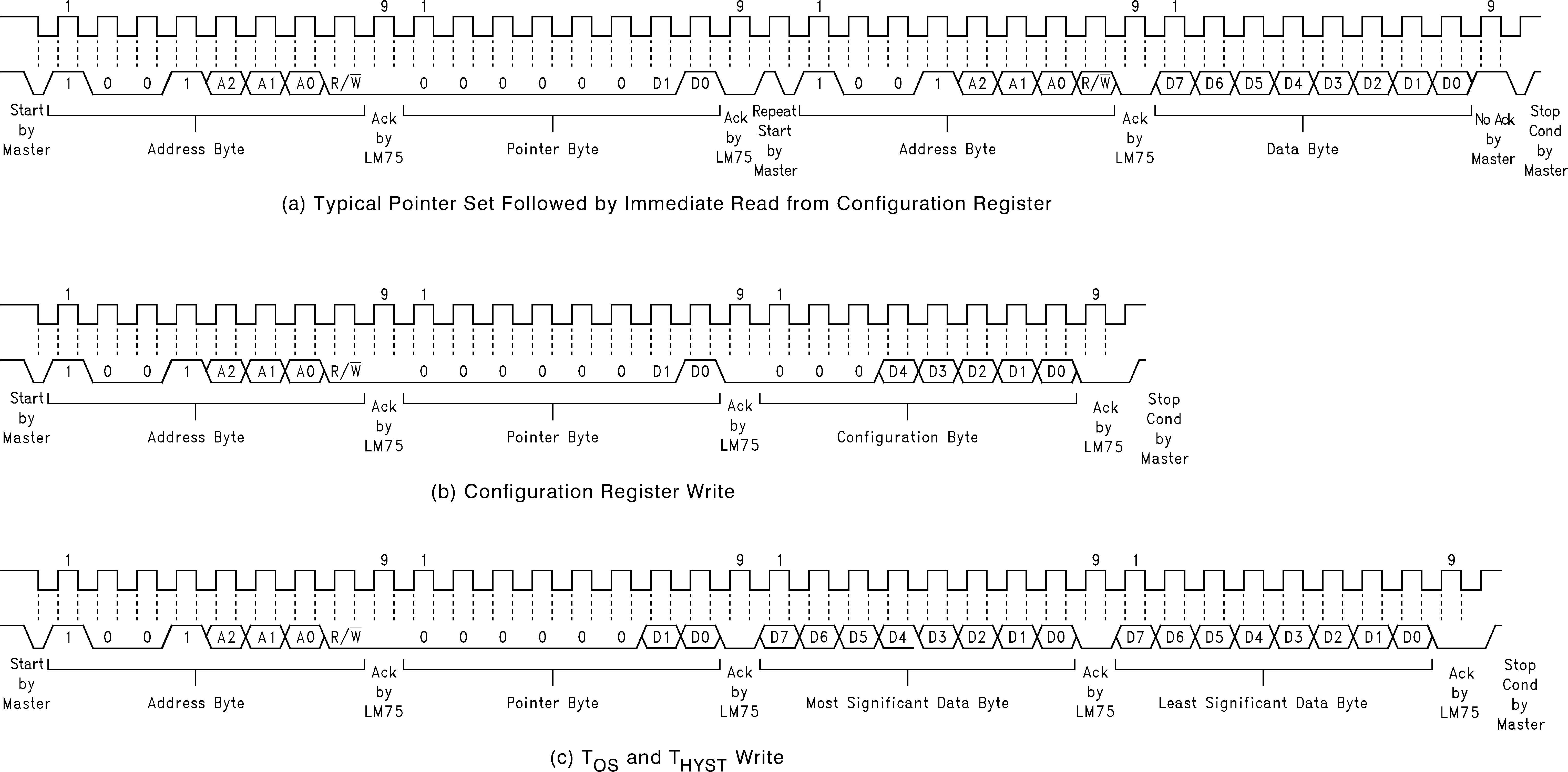 Figure 5. I2C Timing Diagrams (Continued)
6.8 Typical Characteristics
 Figure 6. Accuracy vs Temperature (LM75A)
7 Detailed Description
7.1 Overview
The LM75A temperature sensor incorporates a band-gap type temperature sensor and 9-bit ADC (sigma-delta ADC). The temperature data output of the LM75A is available at all times via the I2C bus. If a conversion is in progress, it will be stopped and restarted after the read. A digital comparator is also incorporated that compares a series of readings, the number of which is user-selectable, to user-programmable setpoint and hysteresis values. The comparator trips the O.S. output line, which is programmable for mode and polarity. The LM75A has an integrated low-pass filter on both the SDA and the SCL line. These filters increase communications reliability in noisy environments.
The LM75A also has a bus fault timeout feature. If the SDA line is held low for longer than tTIMEOUT (see specification) the LM75A will reset to the IDLE state (SDA set to high impedance) and wait for a new start condition. The TIMEOUT feature is not functional in Shutdown Mode.
7.2 Functional Block Diagram

7.3 Feature Description
7.3.1 Digital Temperature Sensor
The LM75A is an industry-standard digital temperature sensor with an integrated sigma-delta ADC and I2C interface. The LM75A provides 9-bit digital temperature readings with an accuracy of ±2°C from –25°C to 100°C and ±3°C over –55°C to 125°C.
The LM75A operates with a single supply from +2.7 V to +5.5 V. Communication is accomplished over a 2-wire interface which operates up to 400kHz. The LM75A has three address pins, allowing up to eight LM75A devices to operate on the same 2-wire bus. The LM75A has a dedicated over-temperature output (O.S.) with programmable limit and hysteresis. This output has programmable fault tolerance, which allows the user to define the number of consecutive error conditions that must occur before O.S. is activated.
7.4 Device Functional Modes
In Comparator mode the O.S. Output behaves like a thermostat. The output becomes active when temperature exceeds the TOS limit, and leaves the active state when the temperature drops below the THYST limit. In this mode the O.S. output can be used to turn a cooling fan on, initiate an emergency system shutdown, or reduce system clock speed. Shutdown mode does not reset O.S. state in a comparator mode.
In Interrupt mode exceeding TOS also makes O.S. active but O.S. will remain active indefinitely until reset by reading any register via the I2C interface. Once O.S. has been activated by crossing TOS, then reset, it can be activated again only by Temperature going below THYST. Again, it will remain active indefinitely until being reset by a read. Placing the LM75A in shutdown mode also resets the O.S. Output.
The LM75A always powers up in a known state. The power up default conditions are:
- Comparator mode
- TOS = 80°C
- THYST = 75°C
- O.S. active low
- Pointer = “00”
When the supply voltage is less than about 1.7V, the LM75A is considered powered down. As the supply voltage rises above the nominal 1.7V power up threshold, the internal registers are reset to the power up default values listed above.
If the LM75A is not connected to the I2C bus on power up, it will act as a stand-alone thermostat with the power up default conditions listed above. It is optional, but recommended, to connect the address pins (A2, A1, A0) and the SCL and SDA pins together and to a 10k pullup resistor to +VS for better noise immunity. Any of these pins may also be tied high separately through a 10-k pullup resistor.
7.5 Programming
7.5.1 I2C Bus Interface
The LM75A operates as a slave on the I2C bus, so the SCL line is an input (no clock is generated by the LM75A) and the SDA line is a bi-directional serial data path. According to I2C bus specifications, the LM75A has a 7-bit slave address. The four most significant bits of the slave address are hard wired inside the LM75A and are “1001”. The three least significant bits of the address are assigned to pins A2–A0, and are set by connecting these pins to ground for a low, (0); or to +VS for a high, (1).
Therefore, the complete slave address is:
| 1 | 0 | 0 | 1 | A2 | A1 | A0 |
|---|---|---|---|---|---|---|
| MSB | LSB | |||||

7.5.2 Temperature Data Format
Temperature data can be read from the Temperature, TOS Set Point, and THYST Set Point registers; and written to the TOS Set Point, and THYST Set Point registers. Temperature data is represented by a 9-bit, two's complement word with an LSB (Least Significant Bit) equal to 0.5°C:
| Temperature | Digital Output | |
|---|---|---|
| Binary | Hex | |
| +125°C | 0 1111 1010 | 0FAh |
| +25°C | 0 0011 0010 | 032h |
| +0.5°C | 0 0000 0001 | 001h |
| 0°C | 0 0000 0000 | 000h |
| −0.5°C | 1 1111 1111 | 1FFh |
| −25°C | 1 1100 1110 | 1CEh |
| −55°C | 1 1001 0010 | 192h |
7.5.3 Shutdown Mode
Shutdown mode is enabled by setting the shutdown bit in the Configuration register via the I2C bus. Shutdown mode reduces power supply current significantly. See specified quiescent current specification in the electrical tables. In Interrupt mode O.S. is reset if previously set and is undefined in Comparator mode during shutdown. The I2C interface remains active. Activity on the clock and data lines of the I2C bus may slightly increase shutdown mode quiescent current. TOS, THYST, and Configuration registers can be read from and written to in shutdown mode.
For the LM75A, the TIMEOUT feature is turned off in Shutdown Mode.
7.5.4 Fault Queue
A fault queue of up to 6 faults is provided to prevent false tripping of O.S. when the LM75A is used in noisy environments. The number of faults set in the queue must occur consecutively to set the O.S. output.
7.5.5 Comparator and Interrupt Mode
As indicated in the O.S. Output Temperature Response Diagram, Figure 7, the events that trigger O.S. are identical for either Comparator or Interrupt mode. The most important difference is that in Interrupt mode the O.S. will remain set indefinitely once it has been set. To reset O.S. while in Interrupt mode, perform a read from any register in the LM75A.
7.5.6 O.S. Output
The O.S. output is an open-drain output and does not have an internal pullup. A “high” level will not be observed on this pin until pullup current is provided from some external source, typically a pullup resistor. Choice of resistor value depends on many system factors but, in general, the pullup resistor should be as large as possible. This will minimize any errors due to internal heating of the LM75A. The maximum resistance of the pullup, based on LM75A specification for High Level Output Current, to provide a 2-V high level, is 30 kΩ.
7.5.7 O.S. Polarity
The O.S. output can be programmed via the configuration register to be either active low (default mode), or active high. In active low mode the O.S. output goes low when triggered exactly as shown on the O.S. Output Temperature Response Diagram, Figure 7. Active high simply inverts the polarity of the O.S. output.
7.5.8 Internal Register Structure
 Figure 8. Register Structure
There are four data registers in the LM75A and an additional Product ID register selected by the Pointer register. At power-up the Pointer is set to “000”; the location for the Temperature Register. The Pointer register latches whatever the last location it was set to. In Interrupt Mode, a read from the LM75A, or placing the device in shutdown mode, resets the O.S. output. All registers are read and write, except the Temperature register and the LM75A's Product ID register, which are read-only.
A write to the LM75A will always include the address byte and the Pointer byte. A write to the Configuration register requires one data byte, and the TOS and THYST registers require two data bytes.
Reading the LM75A can take place either of two ways: If the location latched in the Pointer is correct (most of the time it is expected that the Pointer will point to the Temperature register because it will be the data most frequently read from the LM75A), then the read can simply consist of an address byte, followed by retrieving the corresponding number of data bytes. If the Pointer needs to be set, then an address byte, pointer byte, repeat start, and another address byte will accomplish a read.
The first data byte is the most significant byte with most significant bit first, permitting only as much data as necessary to be read to determine temperature condition. For instance, if the first four bits of the temperature data indicates an overtemperature condition, the host processor could immediately take action to remedy the excessive temperatures. At the end of a read, the LM75A can accept either Acknowledge or No Acknowledge from the Master (No Acknowledge is typically used as a signal for the slave that the Master has read its last byte).
7.6 Register Maps
7.6.1 Pointer Register (Selects Which Registers Will Be Read From or Written to):
| P7 | P6 | P5 | P4 | P3 | P2 | P1 | P0 |
|---|---|---|---|---|---|---|---|
| 0 | 0 | 0 | 0 | 0 | Register Select | ||
P0-P1: Register Select:
| P2 | P1 | P0 | Register |
|---|---|---|---|
| 0 | 0 | 0 | Temperature (Read-only) (Power-up default) |
| 0 | 0 | 1 | Configuration (Read/Write) |
| 0 | 1 | 0 | THYST (Read/Write) |
| 0 | 1 | 1 | TOS (Read/Write) |
| 1 | 1 | 1 | Product ID Register |
P3–P7: Must be kept zero.
7.6.2 Temperature Register (Read-Only):
| D15 | D14 | D13 | D12 | D11 | D10 | D9 | D8 | D7 | D6 | D5 | D4 | D3 | D2 | D1 | D0 |
|---|---|---|---|---|---|---|---|---|---|---|---|---|---|---|---|
| MSB | Bit 7 | Bit 6 | Bit 5 | Bit 4 | Bit 3 | Bit 2 | Bit 1 | LSB | X | X | X | X | X | X | X |
D0–D6: Undefined. D7–D15: Temperature Data. One LSB = 0.5°C. Two's complement format.
7.6.3 Configuration Register (Read/Write):
| D7 | D6 | D5 | D4 | D3 | D2 | D1 | D0 |
|---|---|---|---|---|---|---|---|
| 0 | 0 | 0 | Fault Queue | O.S. Polarity | Cmp/Int | Shutdown | |
Power up default is with all bits “0” (zero).
D0: Shutdown: When set to 1 the LM75A goes to low power shutdown mode.
D1: Comparator/Interrupt mode: 0 is Comparator mode, 1 is Interrupt mode.
D2: O.S. Polarity: 0 is active low, 1 is active high. O.S. is an open-drain output under all conditions.
D3–D4: Fault Queue: Number of faults necessary to detect before setting O.S. output to avoid false tripping due to noise. Faults are determine at the end of a conversion. See specified temperature conversion time in the electrical tables.
| D4 | D3 | Number of Faults |
|---|---|---|
| 0 | 0 | 1 (Power-up default) |
| 0 | 1 | 2 |
| 1 | 0 | 4 |
| 1 | 1 | 6 |
D5–D7: These bits are used for production testing and must be kept zero for normal operation.
7.6.4 THYST and TOS Register (Read/Write):
| D15 | D14 | D13 | D12 | D11 | D10 | D9 | D8 | D7 | D6 | D5 | D4 | D3 | D2 | D1 | D0 |
|---|---|---|---|---|---|---|---|---|---|---|---|---|---|---|---|
| MSB | Bit 7 | Bit 6 | Bit 5 | Bit 4 | Bit 3 | Bit 2 | Bit 1 | LSB | X | X | X | X | X | X | X |
D0–D6: Undefined D7–D15: THYST Or TOS Trip Temperature Data. Power up default is TOS = 80°C, THYST = 75°C
7.6.5 PRODID: Product ID Register (Read-Only) Pointer Address: 07h
| D7 | D6 | D5 | D4 | D3 | D2 | D1 | D0 |
|---|---|---|---|---|---|---|---|
| 1 | 0 | 1 | 0 | 0 | 0 | 0 | 1 |
D4--D7 Product Identification Nibble. Always returns Ah to uniquely identify this part as the LM75A.
D0--D3 Die Revision Nibble. Returns 1h to uniquely identify the revision level as one.