SNOSD63 June 2017 LMH6624-MIL
PRODUCTION DATA.
- 1 Features
- 2 Applications
- 3 Description
- 4 Revision History
- 5 Pin Configuration and Functions
- 6 Specifications
- 7 Detailed Description
- 8 Application and Implementation
- 9 Power Supply Recommendations
- 10Layout
- 11Device and Documentation Support
- 12Mechanical, Packaging, and Orderable Information
Package Options
Mechanical Data (Package|Pins)
- Y|0
Thermal pad, mechanical data (Package|Pins)
Orderable Information
1 Features
- VS = ±6 V, TA = 25°C, AV = 20 (Typical Values Unless Specified)
- Gain Bandwidth 1.5 GHz
- Input Voltage Noise 0.92 nV/√Hz
- Input Offset Voltage (Limit Over Temp) 700 µV
- Slew Rate 350 V/μs
- Slew Rate (AV = 10) 400 V/μs
- HD2 at f = 10 MHz, RL = 100 Ω –63 dBc
- HD3 at f = 10 MHz, RL = 100 Ω –80 dBc
- Supply Voltage Range 5 V to 12 V
- Improved Replacement for the CLC425
- Stable for Closed Loop |AV| ≥ 10
2 Applications
- Instrumentation Sense Amplifiers
- Ultrasound Preamplifiers
- Magnetic Tape & Disk Preamplifers
- Wide Band Active Filters
- Professional Audio Systems
- Opto-Electronics
- Medical Diagnostic Systems
3 Description
The LMH6624-MIL device offers wide bandwidth (1.5 GHz) with very-low-input noise (0.92 nV/√Hz, 2.3 pA/√Hz) and ultra-low DC errors (100-μV VOS, ±0.1-μV/°C drift) providing very precise operational amplifiers with wide dynamic range. This enables the user to achieve closed-loop gains of greater than 10, in both inverting and non-inverting configurations.
The LMH6624-MIL traditional voltage feedback topology provides the following benefits: balanced inputs, low-offset voltage and offset current, very-low-offset drift, 81-dB open loop gain, 95-dB common-mode rejection ratio, and 88-dB power supply rejection ratio.
The LMH6624-MIL device operates from 5 V to 12 V and is offered in SOT-23-5 and SOIC-8 packages.
Device Information(1)
| PART NUMBER | PACKAGE | BODY SIZE (NOM) |
|---|---|---|
| LMH6624-MIL | SOT-23 (5) | 2.90 mm × 1.60 mm |
| SOIC (8) | 4.90 mm × 3.91 mm |
- For all available packages, see the orderable addendum at the end of the datasheet.
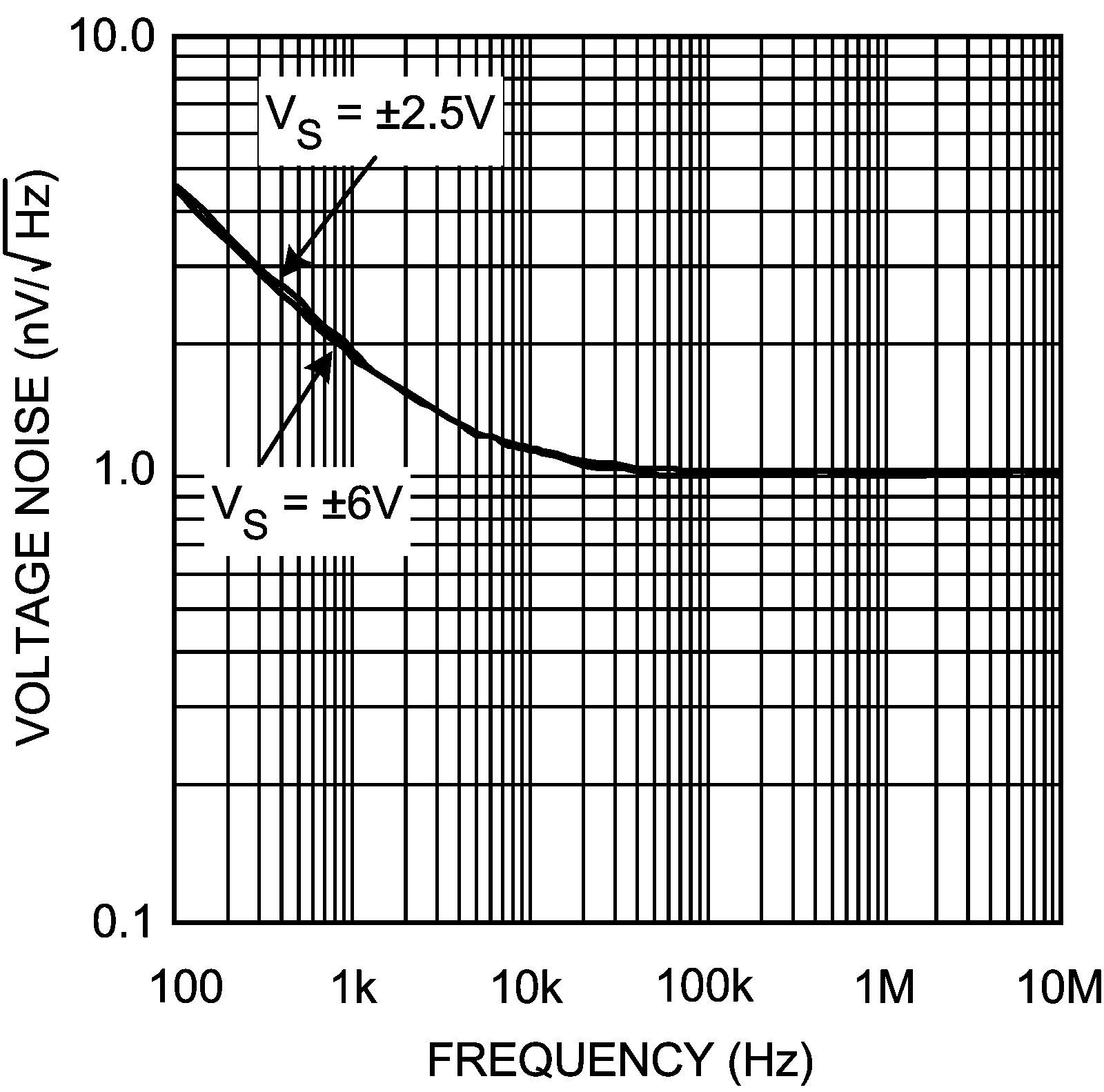
Voltage Noise vs. Frequency
