-
LMH6657 and LMH6658 270-MHz Single Supply, Single and Dual Amplifiers
- 1 Features
- 2 Applications
- 3 Description
- 4 Revision History
- 5 Pin Configuration and Functions
- 6 Specifications
- 7 Detailed Description
- 8 Application and Implementation
- 9 Power Supply Recommendations
- 10Layout
- 11Device and Documentation Support
- 12Mechanical, Packaging, and Orderable Information
- IMPORTANT NOTICE
Package Options
Mechanical Data (Package|Pins)
Thermal pad, mechanical data (Package|Pins)
Orderable Information
LMH6657 and LMH6658 270-MHz Single Supply, Single and Dual Amplifiers
1 Features
- −3dB BW (AV = +1) 270 MHz
- Supply Voltage Range 3 V to 12 V
- Slew Rate, (VS = ±5 V) 700 V/µs
- Supply Current 6.2 mA/amp
- Output Current +80/−90 mA
- Input Common-Mode Volt. 0.5 V Beyond V−, 1.7 V from V+
- Output Voltage Swing (RL = 2 kΩ) 0.8 V from Rails
- Input Voltage Noise 11 nV/√Hz
- Input Current Noise 2.1 pA√Hz/
- DG Error 0.03%
- DP Error 0.10°
- THD (5MHz) −55 dBc
- Settling Time (0.1%) 37ns
- Fully Characterized for 5 V, and ±5 V
- Output Overdrive Recovery 18 ns
- Output Short Circuit Protected(1)
- No Output Phase Reversal With CMVR Exceeded
VS = 5 V, TA = 25°C, RL = 100 Ω (Typical Values Unless Specified)
2 Applications
- CD/DVD ROM
- ADC Buffer Amps
- Portable Video
- Current Sense Buffers
- Portable Communications
(1) Short Circuit Test is a momentary test.
See Note 3 under Absolute Maximum Ratings.
3 Description
The LMH6657 and LMH6658 devices are low-cost operational amplifiers that operate from a single supply with input voltage range extending below the V−. Based on easy to use voltage feedback topology and boasting fast slew rate (700 V/µs) and high speed (140 MHz GBWP), the LMH6657 (Single) and LMH6658 (dual) can be used in high speed large signal applications. These applications include instrumentation, communication devices, set-top boxes, and so forth.
With a -3dB BW of 100 MHz (AV = +2) and DG & DP of 0.03% & 0.10° respectively, the LMH6657 and LMH6658 are well suited for video applications. The output stage can typically supply 80 mA into the load with a swing of about 1 V from either rail.
For Industrial applications, the LMH6657 and LMH6658 are excellent cost-saving choices. Input referred voltage noise is low and the input voltage can extend below V− to ease amplification of low level signals that could be at or near the system ground. With low distortion and fast settling, LMH6657 and LMH6658 can provide buffering for A/D and D/A applications.
The LMH6657 and LMH6658 versatility and ease of use is extended even further by offering these high slew rate, high-speed operational amplifiers in miniature packages such as SOT-23-5, SC70, SOIC-8, and VSSOP-8.
Device Information(1)
| PART NUMBER | PACKAGE | BODY SIZE (NOM) |
|---|---|---|
| LMH6657 | SC70 (5) | 2.00 mm × 1.25 mm |
| SOT-23 (5) | 2.90 mm × 1.60 mm | |
| LMH6658 | SOIC (8) | 4.90 mm × 3.91 mm |
| VSSOP (8) | 3.00 mm × 3.00 mm |
- For all available packages, see the orderable addendum at the end of the data sheet.
Noninverting Frequency Response, Gain

Noninverting Frequency Response, Phase

4 Revision History
Changes from F Revision (April 2013) to G Revision
- Added Pin Configuration and Functions section, ESD Ratings table, Feature Description section, Device Functional Modes, Application and Implementation section, Power Supply Recommendations section, Layout section, Device and Documentation Support section, and Mechanical, Packaging, and Orderable Information section Go
Changes from E Revision (March 2013) to F Revision
- Changed layout of National Data Sheet to TI formatGo
5 Pin Configuration and Functions
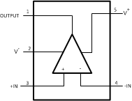
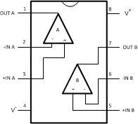
Pin Functions
| PIN | I/O | DESCRIPTION | ||
|---|---|---|---|---|
| NAME | NO. | |||
| SOT-23 AND SC70 |
SOIC AND VSSOP | |||
| OUTPUT | 1 | — | O | Output |
| –IN | 4 | — | I | Inverting input |
| +IN | 3 | — | I | Noninverting input |
| OUT A | — | 1 | O | Output A |
| –IN A | — | 2 | I | Inverting input A |
| +IN A | — | 3 | I | Noninverting input A |
| V– | 2 | 4 | I | Negative Supply |
| OUT B | — | 7 | O | Output B |
| –IN B | — | 6 | I | Inverting input channel B |
| +IN B | — | 5 | I | Noninverting input channel B |
| V+ | 5 | 8 | I | Positive supply |
6 Specifications
6.1 Absolute Maximum Ratings
over operating free-air temperature range (unless otherwise noted)(1)| MIN | MAX | UNIT | ||
|---|---|---|---|---|
| VIN Differential | ±2.5 | V | ||
| Output Short Circuit Duration | See (2)(4) | |||
| Input Current | ±10 | mA | ||
| Supply Voltage (V+ - V−) | 12.6 | V | ||
| Voltage at Input/Output pins | V− − 0.8 | V+ + 0.8 | V | |
| Soldering Information | Infrared or Convection (20 sec.) | 260 | °C | |
| Wave Soldering (10 sec.) | 260 | |||
| Storage temperature, Tstg | –65 | 100 | °C | |
| Junction Temperature(3) | 150 | °C | ||
6.2 ESD Ratings
| VALUE | UNIT | |||
|---|---|---|---|---|
| V(ESD) | Electrostatic discharge | Human body model (HBM), per ANSI/ESDA/JEDEC JS-001(1)(3) | ±2000 | V |
| Machine Model(2) | ±200 | |||
6.3 Recommended Operating Conditions
over operating free-air temperature range (unless otherwise noted)| MIN | MAX | UNIT | ||
|---|---|---|---|---|
| Supply Voltage (V+ – V−) | 3 | 12 | V | |
| Operating Temperature(2) | −40 | 85 | °C | |
6.4 Thermal Information
| THERMAL METRIC(1) | LMH6657 | LMH6658 | UNIT | |||
|---|---|---|---|---|---|---|
| DBV (SOT-23) | DCK (SC70) | D (SOIC) | DGK (VSSOP) | |||
| 5 PINS | 8 PINS | |||||
| RθJA | Junction-to-ambient thermal resistance(2) | 265 | 478 | 190 | 235 | °C/W |
6.5 Electrical Characteristics, 5 V
Unless otherwise specified, all limits ensured for at TJ = 25°C, V+ = 5 V, V− = 0 V, VCM = VO = V+/2, and RL = 100Ω (or as specified) tied to V+/2.| PARAMETER | TEST CONDITIONS | MIN(1) | TYP(2) | MAX(1) | UNIT | ||
|---|---|---|---|---|---|---|---|
| GB | Gain Bandwidth Product | VOUT < 200 mVPP | 140 | MHz | |||
| SSBW | −3-dB BW | AV = +1, VOUT = 200 mVPP | 220 | 270 | MHz | ||
| AV = +2 or −1, VOUT = 200 mVPP | 100 | ||||||
| GFP | Frequency Response Peaking | AV = +2, VOUT = 200 mVPP, DC to 100 MHz |
1.5 | dB | |||
| GFR | Frequency Response Rolloff | AV = +2, VOUT = 200 mVPP, DC to 100 MHz |
0.5 | dB | |||
| LPD1° | 1° Linear Phase Deviation | AV = +2, VOUT = 200 mVPP, ±1° | 30 | MHz | |||
| GF0.1dB | 0.1-dB Gain Flatness | AV = +2, ±0.1 dB, VOUT = 200 mVPP | 13 | MHz | |||
| PBW | Full Power Bandwidth | −1 dB, VOUT = 3 VPP, AV = −1 | 55 | MHz | |||
| DG | Differential Gain | NTSC, VCM = 2 V, RL = 150 Ω to V+/2, Pos. Video Only | 0.03% | ||||
| DP | Differential Phase | NTSC, VCM = 2 V, RL=150 Ω to V+/2 Pos. Video Only | 0.1 | deg | |||
| TIME DOMAIN RESPONSE | |||||||
| tr | Rise and Fall Time | AV = +2, VOUT = 500 mVPP | 3.3 | ns | |||
| AV = −1, VOUT = 500 mVPP | 3.4 | ||||||
| OS | Overshoot, Undershoot | AV = +2, VOUT = 500 mVPP | 18% | ||||
| ts | Settling Time | VO = 2 VPP, ±0.1%, RL = 500 Ω to V+/2, AV = −1 | 37 | ns | |||
| SR | Slew Rate(3) | AV = −1, VO = 3VPP(4) | 470 | V/µs | |||
| AV = +2, VO = 3VPP(4) | 420 | ||||||
| DISTORTION AND NOISE RESPONSE | |||||||
| HD2 | 2nd Harmonic Distortion | f = 5MHz, VO = 2VPP, AV = -1 | −70 | dBc | |||
| HD3 | 3rd Harmonic Distortion | f = 5MHz, VO = 2VPP, AV = -1 | −57 | dBc | |||
| THD | Total Harmonic Distortion | f = 5MHz, VO = 2VPP, AV = -1 | −55.5 | dBc | |||
| Vn | Input-Referred Voltage Noise | f = 100KHz | 11 | nV/√Hz | |||
| f = 1KHz | 19 | ||||||
| In | Input-Referred Current Noise | f = 100KHz | 2.1 | pA/√Hz | |||
| f = 1KHz | 7.5 | ||||||
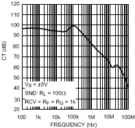
| XTLKA | Cross-Talk Rejection (LMH6658) | f = 5MHz, RL (SND) = 100Ω RCV: RF = RG = 1k |
69 | dB | |||
| STATIC, DC PERFORMANCE | |||||||
| AVOL | Large Signal Voltage Gain | VO = 1.25V to 3.75V, RL = 2k to V+/2 |
85 | 95 | dB | ||
| VO = 1.5V to 3.5V, RL = 150Ω to V+/2 |
75 | 85 | |||||
| VO = 2V to 3V, RL = 50Ω to V+/2 |
70 | 80 | |||||
| CMVR | Input Common-Mode Voltage Range | CMRR ≥ 50dB | −0.2 | −0.5 | V | ||
| At the temperature extremes | −0.1 | ||||||
| 3 | 3.3 | ||||||
| At the temperature extremes | 2.8 | ||||||
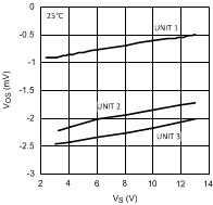
| VOS | Input Offset Voltage | ±1.1 | ±5 | mV | |||
| At the temperature extremes | ±7 | ||||||
| TC VOS | Input Offset Voltage Average Drift | See(6) | ±2 | μV/C | |||
| IB | Input Bias Current | See(5) | −5 | −20 | μA | ||
| At the temperature extremes | −30 | ||||||
| TC IB | Input Bias Current Average Drift | See(6) | 0.01 | nA/°C | |||
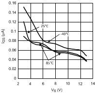
| IOS | Input Offset Current | 50 | 300 | nA | |||
| At the temperature extremes | 500 | ||||||
| CMRR | Common-Mode Rejection Ratio | VCM Stepped from 0V to 3.0V | 72 | 82 | dB | ||
| +PSRR | Positive Power Supply Rejection Ratio | V+ = 4.5V to 5.5V, VCM = 1V | 72 | 82 | dB | ||
| IS | Supply Current (per channel) | No load | 6.2 | 8.5 | mA | ||
| At the temperature extremes | 10 | ||||||
| MISCELLANEOUS PERFORMANCE | |||||||
| VOH | Output Swing High |
RL = 2k to V+/2 | 4.1 | 4.25 | V | ||
| At the temperature extremes | 3.8 | ||||||
| RL = 150Ω to V+/2 | 4 | 4.19 | |||||
| At the temperature extremes | 3.7 | ||||||
| RL = 75Ω to V+/2 | 3.85 | 4.15 | |||||
| At the temperature extremes | 3.5 | ||||||
| VOL | Output Swing Low |
RL = 2k to V+/2 | 900 | 800 | mV | ||
| At the temperature extremes | 1100 | ||||||
| RL = 150Ω to V+/2 | 970 | 870 | |||||
| At the temperature extremes | 1200 | ||||||
| R L = 75Ω to V+/2 | 990 | 885 | |||||
| At the temperature extremes | 1250 | ||||||
| IOUT | Output Current | VOUT = 1V from either rail | Sourcing | 40 | 85 | mA | |
| Sinking | –40 | 105 | |||||
| ISC | Output Short CircuitCurrent(7) | Sourcing to V+/2 | 100 | 155 | mA | ||
| At the temperature extremes | 80 | ||||||
| Sinking to V+/2 | 100 | 220 | |||||
| At the temperature extremes | 80 | ||||||
| RIN | Common-Mode Input Resistance | 3 | MΩ | ||||
| CIN | Common-Mode Input Capacitance | 1.8 | pF | ||||
| ROUT | Output Impedance | f = 1MHz, AV = +1 | 0.06 | Ω | |||
6.6 Electrical Characteristics, ±5 V
Unless otherwise specified, all limits ensured for at TJ = 25°C, V+ = 5 V, V− = −5 V, VCM = VO, and RL = 100 Ω (or as specified) tied to 0 V.| PARAMETER | TEST CONDITIONS | MIN(2) | TYP(1) | MAX(2) | UNIT | ||
|---|---|---|---|---|---|---|---|
| GB | Gain Bandwidth Product | VOUT < 200 mVPP | 140 | MHz | |||
| SSBW | −3-dB BW | AV = +1, VOUT = 200 mVPP | 220 | 270 | MHz | ||
| AV = +2 or −1, VOUT = 200 mVPP | 100 | ||||||
| GFP | Frequency Response Peaking | AV = +2, VOUT = 200 mVPP, DC to 100 MHz |
1 | dB | |||
| GFR | Frequency Response Rolloff | AV = +2, VOUT = 200 mVPP, DC to 100 MHz |
0.9 | dB | |||
| LPD1° | 1° Linear Phase Deviation | AV = +2, VOUT = 200mVPP, ±1° | 30 | MHz | |||
| GF0.1dB | 0.1-dB Gain Flatness | AV = +2, ±0.1 dB, VOUT = 200 mVPP | 20 | MHz | |||
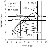
| PBW | Full Power Bandwidth | −1 dB, VOUT = 8 VPP, AV = −1 | 30 | MHz | |||
| DG | Differential Gain | NTSC, RL = 150 Ω, Pos. or Neg. Video | 0.03% | ||||
| DP | Differential Phase | NTSC,RL = 150 Ω, Pos. or Neg. Video | 0.1 | deg | |||
| TIME DOMAIN RESPONSE | |||||||
| tr | Rise and Fall Time | AV = +2, VOUT = 500 mVPP | 3.3 | ns | |||
| AV = −1, VOUT = 500 mVPP | 3.3 | ||||||
| OS | Overshoot, Undershoot | AV = +2, VOUT = 500 mVPP | 16% | ||||
| ts | Settling Time | VO = 5 VPP, ±0.1%, RL =500 Ω, AV = −1 |
35 | ns | |||
| SR | Slew Rate(4) | AV = −1, VO = 8 VPP | 700 | V/µs | |||
| AV = +2, VO = 8 VPP | 500 | ||||||
| DISTORTION AND NOISE RESPONSE | |||||||
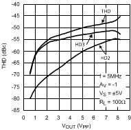
| HD2 | 2nd Harmonic Distortion | f = 5 MHz, VO = 2 VPP, AV = -1 | −70 | dBc | |||
| HD3 | 3rd Harmonic Distortion | f = 5 MHz, VO = 2 VPP, AV = -1 | −57 | dBc | |||
| THD | Total Harmonic Distortion | f = 5 MHz, VO = 2 VPP, AV = -1 | −55.5 | dBc | |||
| Vn | Input-Referred Voltage Noise | f = 100 KHz | 11 | nV/√Hz | |||
| f = 1 KHz | 19 | ||||||
| In | Input-Referred Current Noise | f = 100 KHz | 2.1 | pA/√Hz | |||
| f = 1 KHz | 7.5 | ||||||
| XTLKA | Cross-Talk Rejection (LMH6658) | f = 5 MHz, RL (SND) = 100 Ω RCV: RF = RG = 1 k |
69 | dB | |||
| STATIC, DC PERFORMANCE | |||||||
| AVOL | Large Signal Voltage Gain | VO = −3.75 V to 3.75 V, RL = 2 k | 87 | 100 | dB | ||
| VO = −3.5 V to 3.5 V, RL = 150 Ω | 80 | 90 | |||||
| VO = −3 V to 3 V, RL = 50 Ω | 75 | 85 | |||||
| CMVR | Input Common-Mode Voltage Range | CMRR ≥ 50 dB | −5.2 | −5.5 | V | ||
| At the temperature extremes | −5.1 | ||||||
| 3 | 3.3 | ||||||
| At the temperature extremes | 2.8 | ||||||
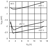
| VOS | Input Offset Voltage | ±1 | ±5 | mV | |||
| Apply at the temperature extremes | ±7 | ||||||
| TC VOS | Input Offset Voltage Average Drift | See (6) | ±2 | μV/C | |||
| IB | Input Bias Current | See (3) | −5 | −20 | μA | ||
| At the temperature extremes | −30 | ||||||
| TCIB | Input Bias Current Average Drift | See (6) | 0.01 | nA/°C | |||
| IOS | Input Offset Current | 50 | 300 | nA | |||
| At the temperature extremes | 500 | ||||||
| CMRR | Common-Mode Rejection Ratio | VCM Stepped from −5 V to 3 V | 75 | 84 | dB | ||
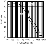
| +PSRR | Positive Power Supply Rejection Ratio | V+ = 4.5 V to 5.5 V, VCM = −4 V | 75 | 82 | dB | ||
| −PSRR | Negative Power Supply Rejection Ratio | V− = −4.5 V to −5.5 V | 78 | 85 | dB | ||
| IS | Supply Current (per channel) | No load | 6.5 | 9 | mA | ||
| At the temperature extremes | 11 | ||||||
| MISCELLANEOUS PERFORMANCE | |||||||
| VOH | Output Swing High |
RL = 2 k | 4.1 | 4.25 | V | ||
| At the temperature extremes | 3.8 | ||||||
| RL = 150 Ω | 4 | 4.2 | |||||
| At the temperature extremes | 3.7 | ||||||
| RL = 75 Ω | 3.85 | 4.18 | |||||
| At the temperature extremes | 3.5 | ||||||
| VOL | Output Swing Low |
RL = 2 k | −4.05 | −4.19 | V | ||
| At the temperature extremes | −3.8 | ||||||
| RL = 150 Ω | −3.9 | −4.05 | |||||
| At the temperature extremes | −3.65 | ||||||
| R L = 75 Ω | −3.8 | −4 | |||||
| At the temperature extremes | −3.5 | ||||||
| IOUT | Output Current | VOUT = 1 V from either rail | Sourcing | 45 | 100 | mA | |
| Sinking | –45 | –110 | |||||
| ISC | Output Short Circuit Current(5) | Sourcing to Ground | 120 | 180 | mA | ||
| At the temperature extremes | 100 | ||||||
| Sinking to Ground | 120 | 230 | |||||
| At the temperature extremes | 100 | ||||||
| RIN | Common-Mode Input Resistance | 4 | MΩ | ||||
| CIN | Common-Mode Input Capacitance | 1.8 | pF | ||||
| ROUT | Output Impedance | f = 1 MHz, AV = +1 | 0.06 | Ω | |||
6.7 Typical Characteristics


