-
LMP202x Zero-Drift, Low-Noise, EMI-Hardened Amplifiers
- 1 Features
- 2 Applications
- 3 Description
- 4 Revision History
- 5 Pin Configuration and Functions SC-70 and VSSOP references from LMP2021 pinout descriptions
- 6 Specifications
- 7 Detailed Description
- 8 Application and Implementation
- 9 Power Supply Recommendations
- 10Layout
- 11Device and Documentation Support
- 12Mechanical, Packaging, and Orderable Information
- IMPORTANT NOTICE
Package Options
Mechanical Data (Package|Pins)
Thermal pad, mechanical data (Package|Pins)
Orderable Information
LMP202x Zero-Drift, Low-Noise, EMI-Hardened Amplifiers
1 Features
- Input Offset Voltage (Typical) −0.4 µV
- Input Offset Voltage (Max) ±5 µV
- Input Offset Voltage Drift (Typical) –0.004 µV/°C
- Input Offset Voltage Drift (Max) ±0.02 µV/°C
- Input Voltage Noise, AV = 1000 11 nV/√Hz
- Open Loop Gain 160 dB
- CMRR 139 dB
- PSRR 130 dB
- Supply Voltage Range 2.2 V to 5.5 V
- Supply Current (per Amplifier) 1.1 mA
- Input Bias Current ±25 pA
- GBW 5 MHz
- Slew Rate 2.6 V/µs
- Operating Temperature Range −40°C to 125°C
- 5-Pin SOT-23, 8-Pin VSSOP and 8-Pin SOIC Packages
(Typical Values, TA = 25°C, VS = 5 V)
2 Applications
- Precision Instrumentation Amplifiers
- Battery Powered Instrumentation
- Thermocouple Amplifiers
- Bridge Amplifiers
3 Description
The LMP2021 and LMP2022 are single and dual precision operational amplifiers offering ultra low input offset voltage, near zero input offset voltage drift, very low input voltage noise and very high open loop gain. They are part of the LMP™ precision family and are ideal for instrumentation and sensor interfaces.
The LMP202x has only 0.004 µV/°C of input offset voltage drift, and 0.4 µV of input offset voltage. These attributes provide great precision in high accuracy applications.
The proprietary continuous auto zero correction circuitry ensures impressive CMRR and PSRR, removes the 1/f noise component, and eliminates the need for calibration in many circuits.
With only 260 nVPP (0.1 Hz to 10 Hz) of input voltage noise and no 1/f noise component, the LMP202x are suitable for low frequency applications such as industrial precision weigh scales. The extremely high open loop gain of 160 dB drastically reduces gain error in high gain applications. With ultra precision DC specifications and very low noise, the LMP202x are ideal for position sensors, bridge sensors, pressure sensors, medical equipment and other high accuracy applications with very low error budgets.
The LMP2021 is offered in 5-Pin SOT-23 and 8-Pin SOIC packages. The LMP2022 is offered in 8-Pin VSSOP and 8-Pin SOIC packages.
Device Information(1)
| PART NUMBER | PACKAGE | BODY SIZE (NOM) |
|---|---|---|
| LMP2021 | SOIC (8) | 4.90 mm x 3.91 mm |
| SOT-23 (5) | 2.90 mm x 1.60 mm | |
| LMP2022 | SOIC (8) | 4.90 mm x 3.91 mm |
| VSSOP (8) | 3.00 mm x 3.00 mm |
- For all available packages, see the orderable addendum at the end of the datasheet.
Bridge Amplifier

4 Revision History
Changes from F Revision (December 2014) to G Revision
- Deleted SC-70 and VSSOP references from LMP2021 pinout descriptions Go
- Deleted DCK and DGK packages and corrected SOT-23 pin function table for LMP2021 Go
Changes from E Revision (March 2013) to F Revision
- Added Pin Configuration and Functions section, ESD Ratings table, Feature Description section, Device Functional Modes, Application and Implementation section, Power Supply Recommendations section, Layout section, Device and Documentation Support section, and Mechanical, Packaging, and Orderable Information section Go
Changes from D Revision (March 2013) to E Revision
- Changed layout of National Data Sheet to TI formatGo
5 Pin Configuration and Functions


Pin Functions: LMP2021
| PIN | I/O | DESCRIPTION | ||||
|---|---|---|---|---|---|---|
| NAME | LMP2021 | |||||
| DBV | D | |||||
| OUT | 1 | 6 | I | Output | ||
| +IN | 3 | 3 | I | Non-Inverting Input | ||
| -IN | 4 | 2 | O | Inverting Input | ||
| V- | 2 | 4 | P | Negative Supply | ||
| V+ | 5 | 7 | P | Positive Supply | ||
| N/C | - | 1 | - | No Internal Connection | ||
| N/C | - | 5 | - | No Internal Connection | ||
| N/C | - | 8 | - | No Internal Connection | ||
Pin Functions: LMP2022
| PIN | I/O | DESCRIPTION | |||
|---|---|---|---|---|---|
| NAME | LMP2022 | ||||
| D, DGK |
|||||
| +IN A | 3 | I | Non-Inverting input, channel A | ||
| +IN B | 5 | I | Non-Inverting input, channel B | ||
| –IN A | 2 | I | Inverting input, channel A | ||
| –IN B | 6 | I | Inverting input, channel B | ||
| OUT A | 1 | O | Output, channel A | ||
| OUT B | 7 | O | Output, channel B | ||
| V+ | 8 | P | Positive (highest) power supply | ||
| V– | 4 | P | Negative (lowest) power supply | ||
6 Specifications
6.1 Absolute Maximum Ratings(1)(2)
| MIN | MAX | UNIT | ||
|---|---|---|---|---|
| VIN Differential | –VS | VS | ||
| Supply Voltage (VS = V+ – V−) | 6.0 | V | ||
| All Other Pins | V+ + 0.3 | V− − 0.3 | V | |
| Output Short-Circuit Duration to V+ or V−(3) | 5 | seconds | ||
| Junction Temperature(4) | 150 | °C | ||
| Soldering Information | Infrared or Convection (20 sec) | 235 | °C | |
| Wave Soldering Lead Temperature (10 sec) | 260 | °C | ||
| Tstg | Storage temperature range | −65 | 150 | °C |
6.2 ESD Ratings
| VALUE | UNIT | |||
|---|---|---|---|---|
| V(ESD) | Electrostatic discharge | Human body model (HBM), per ANSI/ESDA/JEDEC JS-001, all pins(1) | ±2000 | V |
| Charged device model (CDM), per JEDEC specification JESD22-C101, all pins(2) | ±1000 | |||
| Machine model | ±200 | |||
6.3 Recommended Operating Conditions
over operating free-air temperature range (unless otherwise noted)| MIN | MAX | UNIT | ||
|---|---|---|---|---|
| Temperature Range | −40 | 125 | °C | |
| Supply Voltage (VS = V+ – V–) | 2.2 | 5.5 | V | |
6.4 Thermal Information
| THERMAL METRIC(1) | LMP2021, LMP2022 | LMP2021 | LMP2022 | UNIT | |
|---|---|---|---|---|---|
| D | DBV | DGK | |||
| 8 PINS | 5 PINS | 8 PINS | |||
| RθJA | Junction-to-ambient thermal resistance | 106 | 164 | 217 | °C/W |
6.5 Electrical Characteristics: 2.5 V(1)
Unless otherwise specified, all limits are ensured for TA = 25°C, V+ = 2.5 V, V− = 0 V, VCM = V+/2, RL >10 kΩ to V+/2.| PARAMETER | TEST CONDITIONS | MIN(3) | TYP(2) | MAX(3) | UNIT | ||
|---|---|---|---|---|---|---|---|
| VOS | Input Offset Voltage | –5 | –0.9 | 5 | μV | ||
| –40°C ≤ TJ ≤ 125°C | –10 | 10 | |||||
| TCVOS | Input Offset Voltage Drift(4) | –0.02 | 0.001 | 0.02 | μV/°C | ||
| IB | Input Bias Current | –100 | ±23 | 100 | pA | ||
| –40°C ≤ TJ ≤ 125°C | –300 | 300 | |||||
| IOS | Input Offset Current | –200 | ±57 | 200 | pA | ||
| –40°C ≤ TJ ≤ 125°C | –250 | 250 | |||||
| CMRR | Common Mode Rejection Ratio | −0.2 V ≤ VCM ≤ 1.7 V, 0 V ≤ VCM ≤ 1.5 V | 105 | 141 | dB | ||
| −0.2 V ≤ VCM ≤ 1.7 V, 0 V ≤ VCM ≤ 1.5 V, –40°C ≤ TJ ≤ 125°C | 102 | ||||||
| CMVR | Input Common-Mode Voltage Range | Large Signal CMRR ≥ 105 dB | −0.2 | 1.7 | V | ||
| Large Signal CMRR ≥ 102 dB, –40°C ≤ TJ ≤ 125°C | 0 | 1.5 | |||||
| EMIRR | Electro-Magnetic Interference Rejection Ratio(3) | IN+ and IN− | VRF-PEAK = 100 mVP (−20 dBVP) f = 400 MHz |
40 | dB | ||
| VRF-PEAK = 100 mVP (−20 dBVP) f = 900 MHz |
48 | ||||||
| VRF-PEAK = 100 mVP (−20 dBVP) f = 1800 MHz |
67 | ||||||
| VRF-PEAK = 100 mVP (−20 dBVP) f = 2400 MHz |
79 | ||||||
| PSRR | Power Supply Rejection Ratio | 2.5 V ≤ V+ ≤ 5.5 V, VCM = 0 | 115 | 130 | dB | ||
| 2.5 V ≤ V+ ≤ 5.5 V, VCM = 0 , –40°C ≤ TJ ≤ 125°C | 112 | ||||||
| 2.2 V ≤ V+ ≤ 5.5 V, VCM = 0 | 110 | 130 | |||||
| AVOL | Large Signal Voltage Gain | RL = 10 kΩ to V+/2, VOUT = 0.5 V to 2 V | 124 | 150 | dB | ||
| RL = 10 kΩ to V+/2, VOUT = 0.5 V to 2 V, –40°C ≤ TJ ≤ 125°C | 119 | ||||||
| RL = 2 kΩ to V+/2, VOUT = 0.5 V to 2 V | 120 | 150 | |||||
| RL = 2 kΩ to V+/2, VOUT = 0.5 V to 2 V, –40°C ≤ TJ ≤ 125°C | 115 | ||||||
| VOUT | Output Swing High | RL = 10 kΩ to V+/2 | 38 | 50 | mV from either rail |
||
| RL = 10 kΩ to V+/2, –40°C ≤ TJ ≤ 125°C | 70 | ||||||
| RL = 2 kΩ to V+/2 | 62 | 85 | |||||
| RL = 2 kΩ to V+/2, –40°C ≤ TJ ≤ 125°C | 115 | ||||||
| Output Swing Low | RL = 10 kΩ to V+/2 | 30 | 45 | ||||
| RL = 10 kΩ to V+/2, –40°C ≤ TJ ≤ 125°C | 55 | ||||||
| RL = 2 kΩ to V+/2 | 58 | 75 | |||||
| RL = 2 kΩ to V+/2, –40°C ≤ TJ ≤ 125°C | 95 | ||||||
| IOUT | Linear Output Current |
Sourcing, VOUT = 2 V | 30 | 50 | mA | ||
| Sinking, VOUT = 0.5 V | 30 | 50 | |||||
| IS | Supply Current | Per Amplifier | 0.95 | 1.10 | mA | ||
| Per Amplifier, –40°C ≤ TJ ≤ 125°C | 1.37 | ||||||
| SR | Slew Rate(5) | AV = +1, CL = 20 pF, RL = 10 kΩ VO = 2 VPP |
2.5 | V/μs | |||
| GBW | Gain Bandwidth Product | CL = 20 pF, RL = 10 kΩ | 5 | MHz | |||
| GM | Gain Margin | CL = 20 pF, RL = 10 kΩ | 10 | dB | |||
| ΦM | Phase Margin | CL = 20 pF, RL = 10 kΩ | 60 | deg | |||
| CIN | Input Capacitance | Common Mode | 12 | pF | |||
| Differential Mode | 12 | ||||||
| en | Input-Referred Voltage Noise Density | f = 0.1 kHz or 10 kHz, AV = 1000 | 11 | nV/√Hz | |||
| f = 0.1 kHz or 10 kHz, AV = 100 | 15 | ||||||
| Input-Referred Voltage Noise | 0.1 Hz to 10 Hz | 260 | nVPP | ||||
| 0.01 Hz to 10 Hz | 330 | ||||||
| In | Input-Referred Current Noise | f = 1 kHz | 350 | fA/√Hz | |||
| tr | Recovery time | to 0.1%, RL = 10 kΩ, AV = −50, VOUT = 1.25 VPP Step, Duration = 50 μs |
50 | µs | |||
| CT | Cross Talk | LMP2022, f = 1 kHz | 150 | dB | |||
6.6 Electrical Characteristics: 5 V(1)
Unless otherwise specified, all limits are ensured for TA = 25°C, V+ = 5 V, V− = 0 V, VCM = V+/2, RL > 10 kΩ to V+/2.| PARAMETER | TEST CONDITIONS | MIN(3) | TYP(2) | MAX(3) | UNIT | ||
|---|---|---|---|---|---|---|---|
| VOS | Input Offset Voltage | –5 | −0.4 | 5 | μV | ||
| –40°C ≤ TJ ≤ 125°C | –10 | 10 | |||||
| TCVOS | Input Offset Voltage Drift(2) | –0.02 | −0.004 | 0.02 | μV/°C | ||
| IB | Input Bias Current | –100 | ±25 | 100 | pA | ||
| –40°C ≤ TJ ≤ 125°C | –300 | 300 | |||||
| IOS | Input Offset Current | –200 | ±48 | 200 | pA | ||
| –40°C ≤ TJ ≤ 125°C | –250 | 250 | |||||
| CMRR | Common Mode Rejection Ratio | −0.2 V ≤ VCM ≤ 4.2 V, 0 V ≤ VCM ≤ 4.0 V | 120 | 139 | dB | ||
| −0.2 V ≤ VCM ≤ 4.2 V, 0 V ≤ VCM ≤ 4.0 V, –40°C ≤ TJ ≤ 125°C | 115 | ||||||
| CMVR | Input Common-Mode Voltage Range | Large Signal CMRR ≥ 120 dB | –0.2 | 4.2 | V | ||
| Large Signal CMRR ≥ 115 dB, –40°C ≤ TJ ≤ 125°C | 0 | 4.0 | |||||
| EMIRR | Electro-Magnetic Interference Rejection Ratio(3) | IN+ and IN− | VRF-PEAK = 100 mVP (−20 dBVP) f = 400 MHz |
58 | dB | ||
| VRF-PEAK = 100 mVP (−20 dBVP) f = 900 MHz |
64 | ||||||
| VRF-PEAK = 100 mVP (−20 dBVP) f = 1800 MHz |
72 | ||||||
| VRF-PEAK = 100 mVP (−20 dBVP) f = 2400 MHz |
82 | ||||||
| PSRR | Power Supply Rejection Ratio | 2.5 V ≤ V+ ≤ 5.5 V, VCM = 0 | 115 | 130 | dB | ||
| 2.5 V ≤ V+ ≤ 5.5 V, VCM = 0, –40°C ≤ TJ ≤ 125°C | 112 | ||||||
| 2.2 V ≤ V+ ≤ 5.5 V, VCM = 0 | 110 | 130 | |||||
| AVOL | Large Signal Voltage Gain | RL = 10 kΩ to V+/2, VOUT = 0.5 V to 4.5 V | 125 | 160 | dB | ||
| RL = 10 kΩ to V+/2, VOUT = 0.5 V to 4.5 V, –40°C ≤ TJ ≤ 125°C | 120 | ||||||
| RL = 2 kΩ to V+/2, VOUT = 0.5 V to 4.5 V | 123 | 160 | |||||
| RL = 2 kΩ to V+/2, VOUT = 0.5 V to 4.5 V, –40°C ≤ TJ ≤ 125°C | 118 | ||||||
| VOUT | Output Swing High | RL = 10 kΩ to V+/2 | 83 | 135 | mV from either rail |
||
| RL = 10 kΩ to V+/2, –40°C ≤ TJ ≤ 125°C | 170 | ||||||
| RL = 2 kΩ to V+/2 | 120 | 160 | |||||
| RL = 2 kΩ to V+/2, –40°C ≤ TJ ≤ 125°C | 204 | ||||||
| Output Swing Low | RL = 10 kΩ to V+/2 | 65 | 80 | ||||
| RL = 10 kΩ to V+/2, –40°C ≤ TJ ≤ 125°C | 105 | ||||||
| RL = 2 kΩ to V+/2 | 103 | 125 | |||||
| RL = 2 kΩ to V+/2, –40°C ≤ TJ ≤ 125°C | 158 | ||||||
| IOUT | Linear Output Current |
Sourcing, VOUT = 4.5 V | 30 | 50 | mA | ||
| Sinking, VOUT = 0.5 V | 30 | 50 | |||||
| IS | Supply Current | Per Amplifier | 1.1 | 1.25 | mA | ||
| Per Amplifier, –40°C ≤ TJ ≤ 125°C | 1.57 | ||||||
| SR | Slew Rate(4) | AV = +1, CL = 20 pF, RL = 10 kΩ VO = 2 VPP |
2.6 | V/μs | |||
| GBW | Gain Bandwidth Product | CL = 20 pF, RL = 10 kΩ | 5 | MHz | |||
| GM | Gain Margin | CL = 20 pF, RL = 10 kΩ | 10 | dB | |||
| ΦM | Phase Margin | CL = 20 pF, RL = 10 kΩ | 60 | deg | |||
| CIN | Input Capacitance | Common Mode | 12 | pF | |||
| Differential Mode | 12 | ||||||
| en | Input-Referred Voltage Noise Density | f = 0.1 kHz or 10 kHz, AV= 1000 | 11 | nV/√Hz | |||
| f = 0.1 kHz or 10 kHz, AV= 100 | 15 | ||||||
| Input-Referred Voltage Noise | 0.1 Hz to 10 Hz Noise | 260 | nVPP | ||||
| 0.01 Hz to 10 Hz Noise | 330 | ||||||
| In | Input-Referred Current Noise | f = 1 kHz | 350 | fA/√Hz | |||
| tr | Input Overload Recovery time | to 0.1%, RL = 10 kΩ, AV = −50, VOUT = 2.5 VPP Step, Duration = 50 μs |
50 | μs | |||
| CT | Cross Talk | LMP2022, f = 1 kHz | 150 | dB | |||
6.7 Typical Characteristics
Unless otherwise noted: TA = 25°C, RL > 10 kΩ, VS= V+ – V–, VS= 5 V, VCM = VS/2.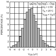 Figure 1. Offset Voltage Distribution
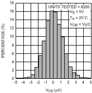 Figure 3. Offset Voltage Distribution
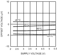 Figure 5. Offset Voltage vs. Supply Voltage
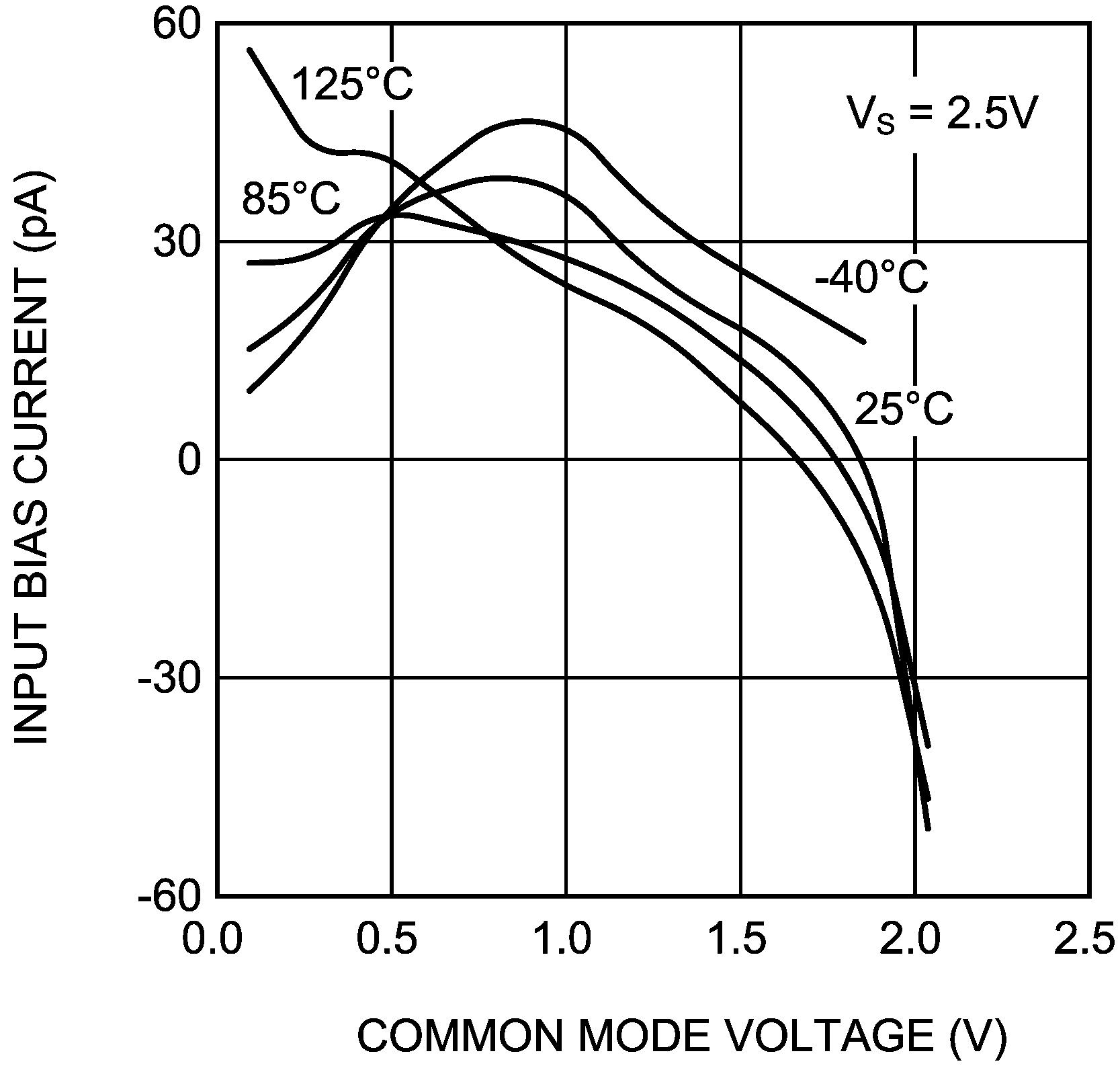 Figure 7. Input Bias Current vs. VCM
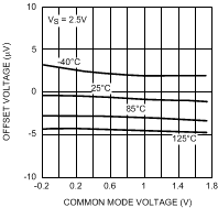 Figure 9. Offset Voltage vs. VCM
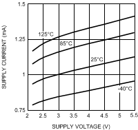 Figure 11. Supply Current vs. Supply Voltage (Per Amplifier)
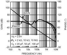 Figure 13. Open Loop Frequency Response
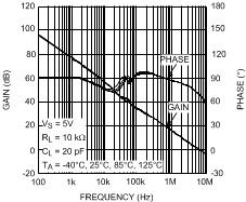 Figure 15. Open Loop Frequency Response Over Temperature
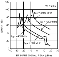 Figure 17. EMIRR vs. Input Power
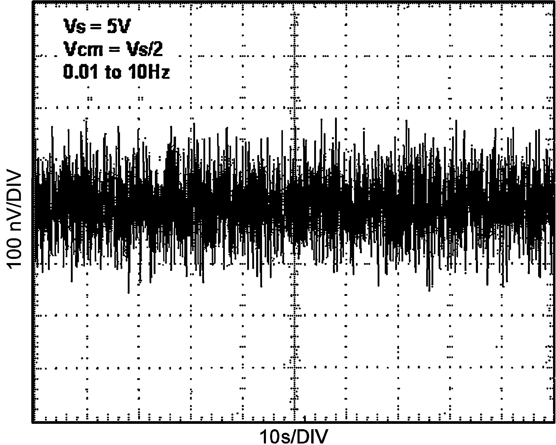 Figure 19. Time Domain Input Voltage Noise
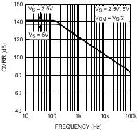 Figure 21. CMRR vs. Frequency
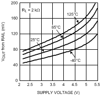 Figure 23. Output Swing High vs. Supply Voltage
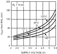 Figure 25. Output Swing High vs. Supply Voltage
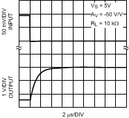 Figure 27. Overload Recovery Time
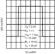 Figure 29. Large Signal Step Response
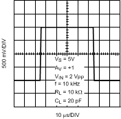 Figure 31. Large Signal Step Response
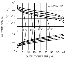 Figure 33. Output Voltage vs. Output Current
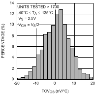 Figure 2. TCVOS Distribution
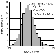 Figure 4. TCVOS Distribution
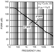 Figure 6. PSRR vs. Frequency
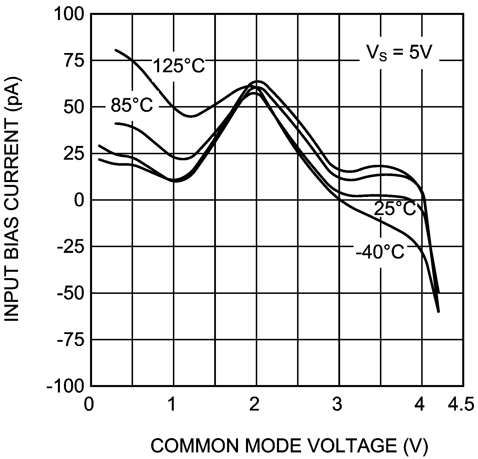 Figure 8. Input Bias Current vs. VCM
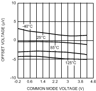 Figure 10. Offset Voltage vs. VCM
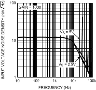 Figure 12. Input Voltage Noise vs. Frequency
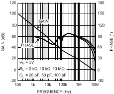 Figure 14. Open Loop Frequency Response
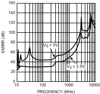 Figure 16. EMIRR vs. Frequency
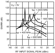 Figure 18. EMIRR vs. Input Power
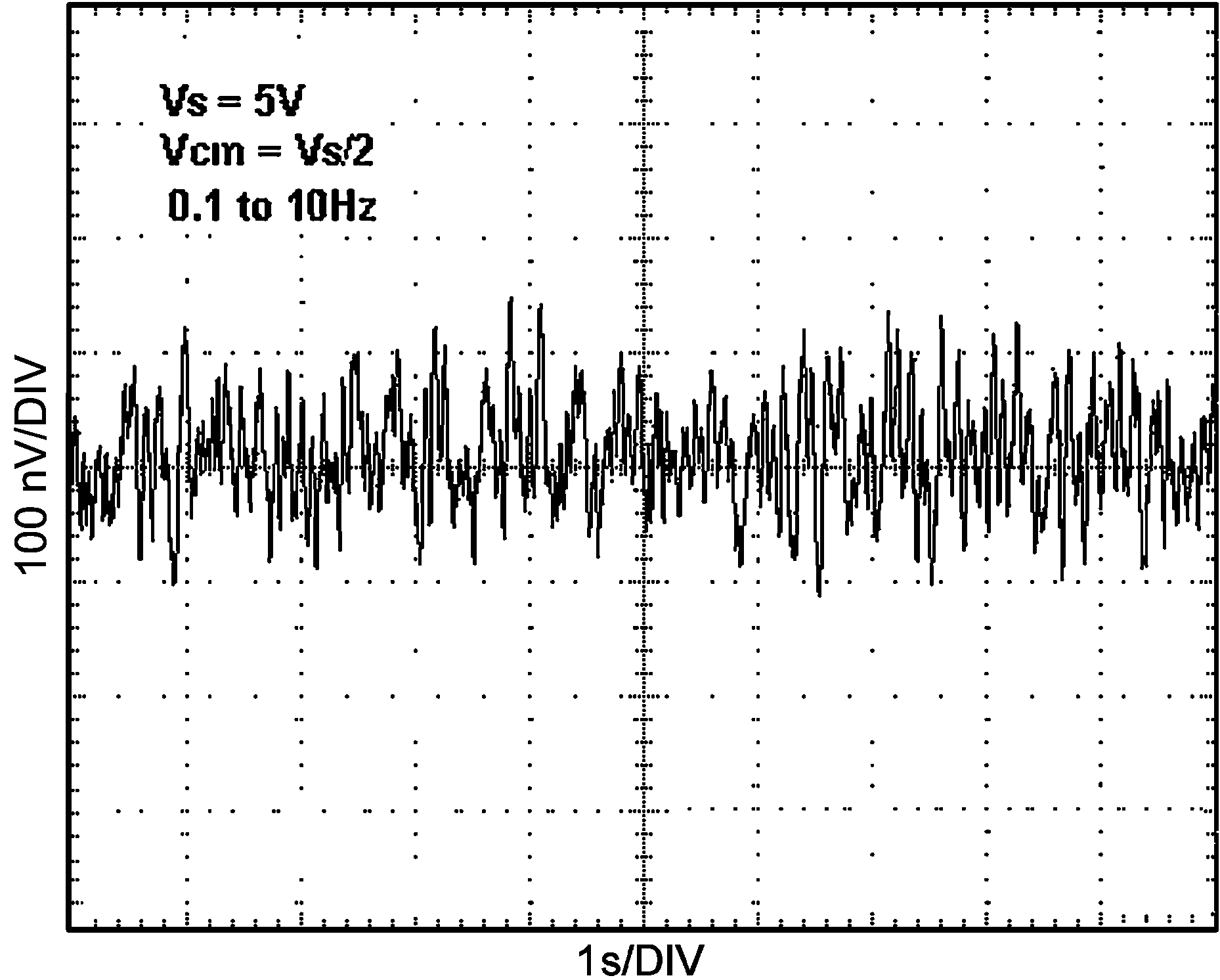 Figure 20. Time Domain Input Voltage Noise
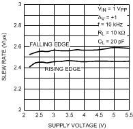 Figure 22. Slew Rate vs. Supply Voltage
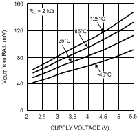 Figure 24. Output Swing Low vs. Supply Voltage
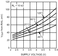 Figure 26. Output Swing Low vs. Supply Voltage
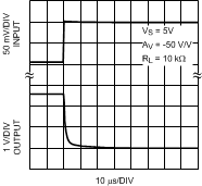 Figure 28. Overload Recovery Time
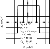 Figure 30. Small Signal Step Response
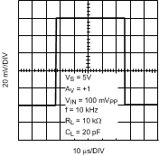 Figure 32. Small Signal Step Response
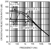 Figure 34. Cross Talk Rejection Ratio vs. Frequency (LMP2022)