The LMP770x are single, dual, and quad low-offset voltage, rail-to-rail input and output precision amplifiers, each with a CMOS input stage and a wide supply voltage range. The LMP770x are part of the LMP™ precision amplifier family and are ideal for sensor interface and other instrumentation applications.
The specified low-offset voltage of less than ±200 µV, along with the specified low input bias current of less than ±1 pA, make the LMP7701 ideal for precision applications. The LMP770x are built using VIP50 technology, which allows the combination of a CMOS input stage and a 12-V common-mode and supply voltage range. This makes the LMP770x ideal for applications where conventional CMOS parts cannot operate under the desired voltage conditions.
PART NUMBER | PACKAGE | BODY SIZE (NOM) |
---|---|---|
LMP7701 | SOT-23 (5) | 1.60 mm × 2.90 mm |
SOIC (8) | 3.91 mm × 4.90 mm | |
LMP7702 | VSSOP (8) | 3.00 mm × 3.00 mm |
SOIC (8) | 3.91 mm × 4.90 mm | |
LMP7704 | TSSOP (14) | 4.40 mm × 5.00 mm |
SOIC (14) | 3.91 mm × 8.65 mm |
Changes from H Revision (March 2013) to I Revision
Changes from G Revision (March 2013) to H Revision
The LMP770x each have a rail-to-rail input stage that significantly reduces the CMRR glitch commonly associated with rail-to-rail input amplifiers. This is achieved by trimming both sides of the complimentary input stage, thereby reducing the difference between the NMOS and PMOS offsets. The output of the LMP770x swings within 40 mV of either rail to maximize the signal dynamic range in applications requiring low supply voltage.
The LMP7701 is offered in the space-saving 5-Pin SOT-23 and 8-Pin SOIC package. The LMP7702 is offered in the 8-Pin SOIC and 8-Pin VSSOP package. The quad LMP7704 is offered in the 14-Pin SOIC and 14-Pin TSSOP package. These small packages are ideal solutions for area constrained PC boards and portable electronics.
PIN | I/O | DESCRIPTION | ||
---|---|---|---|---|
NAME | SOT-23 | SOIC | ||
IN+ | 3 | 3 | I | Noninverting Input |
IN– | 4 | 2 | I | Inverting Input |
IN A + | — | — | I | Noninverting Input for Amplifier A |
IN A– | — | — | I | Inverting Input for Amplifier A |
IN B+ | — | — | I | Noninverting Input for Amplifier B |
IN B– | — | — | I | Inverting Input for Amplifier B |
IN C+ | — | — | I | Noninverting Input for Amplifier C |
IN C– | — | — | I | Inverting Input for Amplifier C |
IN D+ | — | — | I | Noninverting Input for Amplifier D |
IN D– | — | — | I | Inverting Input for Amplifier D |
NC | — | 1, 5, 8 | — | No connection |
OUT | 1 | 6 | O | Output |
OUT A | — | — | O | Output for Amplifier A |
OUT B | — | — | O | Output for Amplifier B |
OUT C | — | — | O | Output for Amplifier C |
OUT D | — | — | O | Output for Amplifier D |
V+ | 5 | 7 | P | Positive Supply |
V– | 2 | 4 | P | Negative Supply |
PIN | I/O | DESCRIPTION | |
---|---|---|---|
NAME | SOIC, VSSOP | ||
IN+ | — | I | Noninverting Input |
IN– | — | I | Inverting Input |
IN A + | 3 | I | Noninverting Input for Amplifier A |
IN A– | 2 | I | Inverting Input for Amplifier A |
IN B+ | 5 | I | Noninverting Input for Amplifier B |
IN B– | 6 | I | Inverting Input for Amplifier B |
IN C+ | — | I | Noninverting Input for Amplifier C |
IN C– | — | I | Inverting Input for Amplifier C |
IN D+ | — | I | Noninverting Input for Amplifier D |
IN D– | — | I | Inverting Input for Amplifier D |
NC | — | — | No connection |
OUT | — | O | Output |
OUT A | 1 | O | Output for Amplifier A |
OUT B | 7 | O | Output for Amplifier B |
OUT C | — | O | Output for Amplifier C |
OUT D | — | O | Output for Amplifier D |
V+ | 8 | P | Positive Supply |
V– | 4 | P | Negative Supply |
PIN | I/O | DESCRIPTION | |
---|---|---|---|
NAME | SOIC, TSSOP | ||
IN+ | — | I | Noninverting Input |
IN– | — | I | Inverting Input |
IN A + | 3 | I | Noninverting Input for Amplifier A |
IN A– | 2 | I | Inverting Input for Amplifier A |
IN B+ | 5 | I | Noninverting Input for Amplifier B |
IN B– | 6 | I | Inverting Input for Amplifier B |
IN C+ | 10 | I | Noninverting Input for Amplifier C |
IN C– | 9 | I | Inverting Input for Amplifier C |
IN D+ | 12 | I | Noninverting Input for Amplifier D |
IN D– | 13 | I | Inverting Input for Amplifier D |
NC | — | — | No connection |
OUT | — | O | Output |
OUT A | 1 | O | Output for Amplifier A |
OUT B | 7 | O | Output for Amplifier B |
OUT C | 8 | O | Output for Amplifier C |
OUT D | 14 | O | Output for Amplifier D |
V+ | 4 | P | Positive Supply |
V– | 11 | P | Negative Supply |
MIN | MAX | UNIT | ||
---|---|---|---|---|
VIN differential | ±300 | mV | ||
Supply voltage (VS = V+ – V−) | 13.2 | V | ||
Voltage at input/output pins | V++ 0.3, V− − 0.3 | V | ||
Input current | 10 | mA | ||
Junction temperature (3) | +150 | °C | ||
Soldering information | Infrared or convection (20 sec) | 235 | °C | |
Wave soldering lead temp. (10 sec) | 260 | °C | ||
Storage temperature, Tstg | −65 | 150 | °C |
VALUE | UNIT | |||
---|---|---|---|---|
V(ESD) | Electrostatic discharge | Human body model (HBM), per ANSI/ESDA/JEDEC JS-001(1)(3) | ±2000 | V |
Charged-device model (CDM), per JEDEC specification JESD22-C101(2) | ±1000 | |||
Machine Model (MM) | ±200 |
MIN | NOM | MAX | UNIT | ||
---|---|---|---|---|---|
Temperature range (2) | −40 | 125 | °C | ||
Supply voltage (VS = V+ – V−) | 2.7 | 12 | V |
THERMAL METRIC(1) | LMP7701 | LMP7701, LMP7702 | LMP7702 | LMP7704 | UNIT | ||
---|---|---|---|---|---|---|---|
DBV (SOT-23) |
D (SOIC) |
DGK (VSSOP) |
D (SOIC) |
PW (TSSOP) |
|||
5 PINS | 8 PINS | 8 PINS | 14 PINS | 14 PINS | |||
RθJA | Junction-to-ambient thermal resistance (2) | 122.9 | 114.3 | 167.5 | 79.9 | 107.5 | °C/W |
RθJC(top) | Junction-to-case (top) thermal resistance | 69.3 | 59.5 | 58.7 | 36.9 | 33.0 | °C/W |
RθJB | Junction-to-board thermal resistance | 63.3 | 54.8 | 87.5 | 34.7 | 50.4 | °C/W |
ψJT | Junction-to-top characterization parameter | 19.4 | 12.1 | 6.6 | 5.5 | 1.8 | °C/W |
ψJB | Junction-to-board characterization parameter | 62.8 | 54.2 | 86.1 | 34.4 | 49.7 | °C/W |
PARAMETER | TEST CONDITIONS | MIN (3) | TYP (2) | MAX (3) | UNIT | ||
---|---|---|---|---|---|---|---|
VOS | Input Offset Voltage | LMP7701 | ±37 | ±200 | μV | ||
at the temperature extremes | ±500 | ||||||
LMP7702/LMP7704 | ±56 | ±220 | |||||
at the temperature extremes | ±520 | ||||||
TCVOS | Input Offset Voltage Temperature Drift | See (4) | ±1 | μV/°C | |||
at the temperature extremes | ±5 | ||||||
IB | Input Bias Current | See (4) (5)
−40°C ≤ TA ≤ 85°C |
±0.2 | ±1 | pA | ||
at the temperature extremes | ±50 | ||||||
See (4) (5)
−40°C ≤ TA ≤ 125°C |
±0.2 | ±1 | |||||
at the temperature extremes | ±400 | ||||||
IOS | Input Offset Current | 40 | fA | ||||
CMRR | Common-Mode Rejection Ratio | 0 V ≤ VCM ≤ 3 V LMP7701 |
86 | 130 | dB | ||
at the temperature extremes | 80 | ||||||
0 V ≤ VCM ≤ 3 V LMP7702/LMP7704 |
84 | 130 | |||||
at the temperature extremes | 78 | ||||||
PSRR | Power Supply Rejection Ratio | 2.7 V ≤ V+ ≤ 12 V, Vo = V+/2 | 86 | 98 | dB | ||
at the temperature extremes | 82 | ||||||
CMVR | Common-Mode Voltage Range | CMRR ≥ 80 dB | –0.2 | 3.2 | V | ||
CMRR ≥ 77 dB | at the temperature extremes | –0.2 | 3.2 | ||||
AVOL | Open-Loop Voltage Gain | RL = 2 kΩ (LMP7701) VO = 0.3 V to 2.7 V |
100 | 114 | dB | ||
at the temperature extremes | 96 | ||||||
RL = 2 kΩ (LMP7702/LMP7704) VO = 0.3 V to 2.7 V |
100 | 114 | |||||
at the temperature extremes | 94 | ||||||
RL = 10 kΩ VO = 0.2 V to 2.8 V |
100 | 124 | |||||
at the temperature extremes | 96 | ||||||
VOUT | Output Voltage Swing High | RL = 2 kΩ to V+/2 LMP7701 |
40 | 80 | mV from V+ |
||
at the temperature extremes | 120 | ||||||
RL = 2 kΩ to V+/2 LMP7702/LMP7704 |
40 | 80 | |||||
at the temperature extremes | 150 | ||||||
RL = 10 kΩ to V+/2 LMP7701 |
30 | 40 | |||||
at the temperature extremes | 60 | ||||||
RL = 10 kΩ to V+/2 LMP7702/LMP7704 |
35 | 50 | |||||
at the temperature extremes | 100 | ||||||
Output Voltage Swing Low | RL = 2 kΩ to V+/2 LMP7701 |
40 | 60 | mV | |||
at the temperature extremes | 80 | ||||||
RL = 2 kΩ to V+/2 LMP7702/LMP7704 |
45 | 100 | |||||
at the temperature extremes | 170 | ||||||
RL = 10 kΩ to V+/2 LMP7701 |
20 | 40 | |||||
at the temperature extremes | 50 | ||||||
RL = 10 kΩ to V+/2 LMP7702/LMP7704 |
20 | 50 | |||||
at the temperature extremes | 90 | ||||||
IOUT | Output Current (8) (6) | Sourcing VO = V+/2 VIN = 100 mV |
25 | 42 | mA | ||
at the temperature extremes | 15 | ||||||
Sinking VO = V+/2 VIN = −100 mV (LMP7701) |
25 | 42 | |||||
at the temperature extremes | 20 | ||||||
Sinking VO = V+/2 VIN = −100 mV (LMP7702/LMP7704) |
25 | 42 | |||||
at the temperature extremes | 15 | ||||||
IS | Supply Current | LMP7701 | 0.670 | 1 | mA | ||
at the temperature extremes | 1.2 | ||||||
LMP7702 | 1.4 | 1.8 | |||||
at the temperature extremes | 2.1 | ||||||
LMP7704 | 2.9 | 3.5 | |||||
at the temperature extremes | 4.5 | ||||||
SR | Slew Rate (7) | AV = +1, VO = 2 VPP
10% to 90% |
0.9 | V/μs | |||
GBW | Gain Bandwidth | 2.5 | MHz | ||||
THD+N | Total Harmonic Distortion + Noise | f = 1 kHz, AV = 1, R.L = 10 kΩ | 0.02% | ||||
en | Input Referred Voltage Noise Density | f = 1 kHz | 9 | nV/√Hz | |||
in | Input Referred Current Noise Density | f = 100 kHz | 1 | fA/√Hz |
PARAMETER | TEST CONDITIONS | MIN (3) | TYP (2) | MAX (3) | UNIT | ||
---|---|---|---|---|---|---|---|
VOS | Input Offset Voltage | LMP7701 | ±37 | ±200 | μV | ||
at the temperature extremes | ±500 | ||||||
LMP7702/LMP7704 | ±32 | ±220 | |||||
at the temperature extremes | ±520 | ||||||
TCVOS | Input Offset Voltage Temperature Drift | See (4) | ±1 | ±5 | μV/°C | ||
at the temperature extremes | |||||||
IB | Input Bias Current | See (4) (5)
−40°C ≤ TA ≤ 85°C |
±0.2 | ±1 | pA | ||
at the temperature extremes | ±50 | ||||||
See (4) (5)
−40°C ≤ TA ≤ 125°C |
±0.2 | ±1 | |||||
at the temperature extremes | ±400 | ||||||
IOS | Input Offset Current | 40 | fA | ||||
CMRR | Common-Mode Rejection Ratio | 0 V ≤ VCM ≤ 5 V LMP7701 |
88 | 130 | dB | ||
at the temperature extremes | 83 | ||||||
0 V ≤ VCM ≤ 5 V LMP7702/LMP7704 |
86 | 130 | |||||
at the temperature extremes | 81 | ||||||
PSRR | Power Supply Rejection Ratio | 2.7 V ≤ V+ ≤ 12 V, VO = V+/2 | 86 | 100 | dB | ||
at the temperature extremes | 82 | ||||||
CMVR | Common-Mode Voltage Range | CMRR ≥ 80 dB | –0.2 | 5.2 | V | ||
CMRR ≥ 78 dB | at the temperature extremes | –0.2 | 5.2 | ||||
AVOL | Open-Loop Voltage Gain | RL = 2 kΩ (LMP7701) VO = 0.3 V to 4.7 V |
100 | 119 | dB | ||
at the temperature extremes | 96 | ||||||
RL = 2 kΩ (LMP7702/LMP7704) VO = 0.3 V to 4.7 V |
100 | 119 | |||||
at the temperature extremes | 94 | ||||||
RL = 10 kΩ VO = 0.2 V to 4.8 V |
100 | 130 | |||||
at the temperature extremes | 96 | ||||||
VOUT | Output Voltage Swing High | RL = 2 kΩ to V+/2 LMP7701 |
60 | 110 | mV from V+ |
||
at the temperature extremes | 130 | ||||||
RL = 2 kΩ to V+/2 LMP7702/LMP7704 |
60 | 120 | |||||
at the temperature extremes | 200 | ||||||
RL = 10 kΩ to V+/2 LMP7701 |
40 | 50 | |||||
at the temperature extremes | 70 | ||||||
RL = 10 kΩ to V+/2 LMP7702/LMP7704 |
40 | 60 | |||||
at the temperature extremes | 120 | ||||||
Output Voltage Swing Low | RL = 2 kΩ to V+/2 LMP7701 |
50 | 80 | mV | |||
at the temperature extremes | 90 | ||||||
RL = 2 kΩ to V+/2 LMP7702/LMP7704 |
50 | 120 | |||||
at the temperature extremes | 190 | ||||||
RL = 10 kΩ to V+/2 LMP7701 |
30 | 40 | |||||
at the temperature extremes | 50 | ||||||
RL = 10 kΩ to V+/2 LMP7702/LMP7704 |
30 | 50 | |||||
at the temperature extremes | 100 | ||||||
IOUT | Output Current (8) (6) | Sourcing VO = V+/2 VIN = 100 mV (LMP7701) |
40 | 66 | mA | ||
at the temperature extremes | 28 | ||||||
Sourcing VO = V+/2 VIN = 100 mV (LMP7702/LMP7704) |
38 | 66 | |||||
at the temperature extremes | 25 | ||||||
Sinking VO = V+/2 VIN = −100 mV (LMP7701) |
40 | 76 | |||||
at the temperature extremes | 28 | ||||||
Sinking VO = V+/2 VIN = −100 mV (LMP7702/LMP7704) |
40 | 76 | |||||
at the temperature extremes | 23 | ||||||
IS | Supply Current | LMP7701 | 0.715 | 1 | mA | ||
at the temperature extremes | 1.2 | ||||||
LMP7702 | 1.5 | 1.9 | |||||
at the temperature extremes | 2.2 | ||||||
LMP7704 | 2.9 | 3.7 | |||||
at the temperature extremes | 4.6 | ||||||
SR | Slew Rate (7) | AV = +1, VO = 4 VPP
10% to 90% |
1 | V/μs | |||
GBW | Gain Bandwidth | 2.5 | MHz | ||||
THD+N | Total Harmonic Distortion + Noise | f = 1 kHz, AV = 1, RL = 10 kΩ | 0.02% | ||||
en | Input Referred Voltage Noise Density | f = 1 kHz | 9 | nV/√Hz | |||
in | Input Referred Current Noise Density | f = 100 kHz | 1 | fA/√Hz |
PARAMETER | TEST CONDITIONS | MIN (3) | TYP (2) | MAX (3) | UNIT | ||
---|---|---|---|---|---|---|---|
VOS | Input Offset Voltage | LMP7701 | ±37 | ±200 | μV | ||
at the temperature extremes | ±500 | ||||||
LMP7702/LMP7704 | ±37 | ±220 | |||||
at the temperature extremes | ±520 | ||||||
TCVOS | Input Offset Voltage Temperature Drift | See (4) | ±1 | μV/°C | |||
at the temperature extremes | ±5 | ||||||
IB | Input Bias Current | See (4) (5)
−40°C ≤ TA ≤ 85°C |
±0.2 | 1 | pA | ||
at the temperature extremes | ±50 | ||||||
See (4) (5)
−40°C ≤ TA ≤ 125°C |
±0.2 | 1 | |||||
at the temperature extremes | ±400 | ||||||
IOS | Input Offset Current | 40 | fA | ||||
CMRR | Common-Mode Rejection Ratio | −5 V ≤ VCM ≤ 5 V LMP7701 |
92 | 138 | dB | ||
at the temperature extremes | 88 | ||||||
−5 V ≤ VCM ≤ 5 V LMP7702/LMP7704 |
90 | 138 | |||||
at the temperature extremes | 86 | ||||||
PSRR | Power Supply Rejection Ratio | 2.7 V ≤ V+ ≤ 12 V, VO = 0 V | 86 | 98 | dB | ||
at the temperature extremes | 82 | ||||||
CMVR | Common-Mode Voltage Range | CMRR ≥ 80 dB | −5.2 | 5.2 | V | ||
CMRR ≥ 78 dB | at the temperature extremes | −5.2 | 5.2 | ||||
AVOL | Open Loop Voltage Gain | RL = 2 kΩ (LMP7701) VO = −4.7 V to 4.7 V |
100 | 121 | dB | ||
at the temperature extremes | 98 | ||||||
RL = 2 kΩ (LMP7702/LMP7704) VO = −4.7 V to 4.7 V |
100 | 121 | |||||
at the temperature extremes | 94 | ||||||
RL = 10 kΩ (LMP7701) VO = −4.8 V to 4.8 V |
100 | 134 | |||||
at the temperature extremes | 98 | ||||||
RL = 10 kΩ (LMP7702/LMP7704) VO = −4.8 V to 4.8 V |
100 | 134 | |||||
at the temperature extremes | 97 | ||||||
VOUT | Output Voltage Swing High | RL = 2 kΩ to 0 V LMP7701 |
90 | 150 | mV from V+ |
||
at the temperature extremes | 170 | ||||||
RL = 2 kΩ to 0 V LMP7702/LMP7704 |
90 | 180 | |||||
at the temperature extremes | 290 | ||||||
RL = 10 kΩ to 0 V LMP7701 |
40 | 80 | |||||
at the temperature extremes | 100 | ||||||
RL = 10 kΩ to 0 V LMP7702/LMP7704 |
40 | 80 | |||||
at the temperature extremes | 150 | ||||||
Output Voltage Swing Low | RL = 2 kΩ to 0 V LMP7701 |
90 | 130 | mV from V– |
|||
at the temperature extremes | 150 | ||||||
RL = 2 kΩ to 0 V LMP7702/LMP7704 |
90 | 180 | |||||
at the temperature extremes | 260 | ||||||
RL = 10 kΩ to 0 V LMP7701 |
40 | 50 | |||||
at the temperature extremes | 60 | ||||||
RL = 10 kΩ to 0 V LMP7702/LMP7704 |
40 | 60 | |||||
at the temperature extremes | 110 | ||||||
IOUT | Output Current (8) (6) | Sourcing VO = 0 V VIN = 100 mV (LMP7701) |
50 | 86 | mA | ||
at the temperature extremes | 35 | ||||||
Sourcing VO = 0 V VIN = 100 mV (LMP7702/LMP7704) |
48 | 86 | |||||
at the temperature extremes | 33 | ||||||
Sinking VO = 0 V VIN = −100 mV |
50 | 84 | |||||
at the temperature extremes | 35 | ||||||
IS | Supply Current | LMP7701 | 0.790 | 1.1 | mA | ||
at the temperature extremes | 1.3 | ||||||
LMP7702 | 1.7 | 2.1 | |||||
at the temperature extremes | 2.5 | ||||||
LMP7704 | 3.2 | 4.2 | |||||
at the temperature extremes | 5 | ||||||
SR | Slew Rate (7) | AV = +1, VO = 9 VPP
10% to 90% |
1.1 | V/μs | |||
GBW | Gain Bandwidth | 2.5 | MHz | ||||
THD+N | Total Harmonic Distortion + Noise | f = 1 kHz, AV = 1, RL = 10 kΩ | 0.02% | ||||
en | Input Referred Voltage Noise Density | f = 1 kHz | 9 | nV/√Hz | |||
in | Input Referred Current Noise Density | f = 100 kHz | 1 | fA/√Hz |
The LMP770x are single, dual, and quad low offset voltage, rail-to-rail input and output precision amplifiers each with a CMOS input stage and wide supply voltage range of 2.7V to 12V. The LMP770x have a very low input bias current of only ±200 fA at room temperature.
The wide supply voltage range of 2.7V to 12V over the extensive temperature range of −40°C to 125°C makes the LMP770x excellent choices for low voltage precision applications with extensive temperature requirements.
The LMP770x have only ±37 μV of typical input referred offset voltage and this offset is specified to be less than ±500 μV for the single and ±520 μV for the dual and quad, over temperature. This minimal offset voltage allows more accurate signal detection and amplification in precision applications.
The low input bias current of only ±200 fA along with the low input referred voltage noise of 9 nV/√Hz gives the LMP770x superiority for use in sensor applications. Lower levels of noise from the LMP770x mean of better signal fidelity and a higher signal-to-noise ratio.
Texas Instruments is heavily committed to precision amplifiers and the market segment they serve. Technical support and extensive characterization data is available for sensitive applications or applications with a constrained error budget.
The LMP7701 is offered in the space saving 5-Pin SOT-23 and 8-Pin SOIC package. The LMP7702 comes in the 8-Pin SOIC and 8-Pin VSSOP package. The LMP7704 is offered in the 14-Pin SOIC and 14-Pin TSSOP package. These small packages are ideal solutions for area constrained PC boards and portable electronics.
The LMP770x can each be connected as a non-inverting unity gain follower. This configuration is the most sensitive to capacitive loading.
The combination of a capacitive load placed on the output of an amplifier along with the amplifier's output impedance creates a phase lag which in turn reduces the phase margin of the amplifier. If the phase margin is significantly reduced, the response will be either underdamped or it will oscillate.
To drive heavier capacitive loads, an isolation resistor, RISO, in Figure 40 should be used. By using this isolation resistor, the capacitive load is isolated from the amplifier's output, and hence, the pole caused by CL is no longer in the feedback loop. The larger the value of RISO, the more stable the output voltage will be. If values of RISO are sufficiently large, the feedback loop will be stable, independent of the value of CL. However, larger values of RISO result in reduced output swing and reduced output current drive.
CMOS input stages inherently have low input bias current and higher input referred voltage noise. The LMP770x enhance this performance by having the low input bias current of only ±200 fA, as well as, a very low input referred voltage noise of 9 nV/√Hz. To achieve this a larger input stage has been used. This larger input stage increases the input capacitance of the LMP770x. The typical value of this input capacitance, CIN, for the LMP770x is 25 pF. The input capacitance will interact with other impedances such as gain and feedback resistors, which are seen on the inputs of the amplifier, to form a pole. This pole will have little or no effect on the output of the amplifier at low frequencies and DC conditions, but will play a bigger role as the frequency increases. At higher frequencies, the presence of this pole will decrease phase margin and will also cause gain peaking. To compensate for the input capacitance, care must be taken in choosing the feedback resistors. In addition to being selective in picking values for the feedback resistor, a capacitor can be added to the feedback path to increase stability.
The DC gain of the circuit shown in Figure 41 is simply –R2/R1.
For the time being, ignore CF. The AC gain of the circuit in Figure 41 can be calculated as follows:
This equation is rearranged to find the location of the two poles:
As shown in Equation 2, as values of R1 and R2 are increased, the magnitude of the poles is reduced, which in turn decreases the bandwidth of the amplifier. Whenever possible, it is best to choose smaller feedback resistors. Figure 42 shows the effect of the feedback resistor on the bandwidth of the LMP770x.
Equation 2 has two poles. In most cases, it is the presence of pairs of poles that causes gain peaking. To eliminate this effect, the poles should be placed in Butterworth position, because poles in Butterworth position do not cause gain peaking. To achieve a Butterworth pair, the quantity under the square root in Equation 2 should be set to equal −1. Using this fact and the relation between R1 and R2, R2 = −AV R1, the optimum value for R1 can be found. This is shown in Equation 3. If R1 is chosen to be larger than this optimum value, gain peaking will occur.
In Figure 41, CF is added to compensate for input capacitance and to increase stability. Additionally, CF reduces or eliminates the gain peaking that can be caused by having a larger feedback resistor. Figure 43 shows how CF reduces gain peaking.
The LMP770x have a set of anti-parallel diodes between the input pins, as shown in Figure 44. These diodes are present to protect the input stage of the amplifier. At the same time, they limit the amount of differential input voltage that is allowed on the input pins. A differential signal larger than one diode voltage drop might damage the diodes. The differential signal between the inputs needs to be limited to ±300 mV or the input current needs to be limited to ±10 mA.
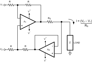
The LMP770x can each be used as a precision current source in many different applications. Figure 45 shows a typical precision current source. This circuit implements a precision voltage controlled current source. Amplifier A1 is a differential amplifier that uses the voltage drop across RS as the feedback signal. Amplifier A2 is a buffer that eliminates the error current from the load side of the RS resistor that would flow in the feedback resistor if it were connected to the load side of the RS resistor. In general, the circuit is stable as long as the closed loop bandwidth of amplifier A2 is greater then the closed loop bandwidth of amplifier A1. If A1 and A2 are the same type of amplifiers, then the feedback around A1 will reduce its bandwidth compared to A2.
The equation for output current can be derived as shown in Equation 4.
Solving for the current I results in the Equation 5.