-
LMV11x Low-Voltage, 45-MHz, Rail-To-Rail Output Operational Amplifiers With Shutdown Option
- 1 Features
- 2 Applications
- 3 Description
- 4 Revision History
- 5 Pin Configuration and Functions
- 6 Specifications
- 7 Detailed Description
- 8 Application and Implementation
- 9 Power Supply Recommendations
- 10Layout
- 11Device and Documentation Support
- 12Mechanical, Packaging, and Orderable Information
- IMPORTANT NOTICE
Package Options
Mechanical Data (Package|Pins)
- DBV|6
Thermal pad, mechanical data (Package|Pins)
Orderable Information
LMV11x Low-Voltage, 45-MHz, Rail-To-Rail Output Operational Amplifiers With Shutdown Option
1 Features
- −3-dB BW 45 MHz
- Supply Voltage Range 2.7 V to 12 V
- Slew Rate 40 V/μs
- Supply Current 600 μA
- Power Down Supply Current 15 μA
- Output Short Circuit Current 32 mA
- Linear Output Current ±20 mA
- Input Common Mode Voltage −0.3 V to 1.7 V
- Output Voltage Swing 20 mV from Rails
- Input Voltage Noise 40 nV/√Hz
- Input Current Noise 0.75 pA/√Hz
2 Applications
- High-Speed Clock Buffer/Driver
- Active Filters
- High-Speed Portable Devices
- Multiplexing Applications (LMV118)
- Current Sense Amplifier
- High-Speed Transducer Amplifier
3 Description
The LMV116 (single) rail-to-rail output voltage feedback amplifiers offer high-speed (45 MHz), and low-voltage operation (2.7 V) in addition to micro-power shutdown capability (LMV118).
Output voltage range extends to within 20 mV of either supply rail, allowing wide dynamic range especially in low voltage applications. Even with low supply current of 600 μA, output current capability is kept at a respectable ±20 mA for driving heavier loads. Important device parameters such as BW, slew rate, and output current are kept relatively independent of the operating supply voltage by a combination of process enhancements and design architecture.
For portable applications, the LMV118 provides shutdown capability while keeping the turnoff current to 15 μA. Both turnon and turnoff characteristics are well behaved with minimal output fluctuations during transitions, thus the device can be used in power-saving mode, as well as multiplexing applications. Miniature packages (5-pin and 6-pin SOT-23) are further means to ease the adoption of these low-power, high-speed devices in applications where board area is at a premium.
Device Information(1)
| PART NUMBER | PACKAGE | BODY SIZE (NOM) |
|---|---|---|
| LMV116 | SOT-23 (5) | 2.90 mm × 1.60 mm |
| SOT-23 (6) | 2.90 mm × 1.60 mm | |
| LMV118 | SOT-23 (5) | 2.90 mm × 1.60 mm |
| SOT-23 (6) | 2.90 mm × 1.60 mm |
- For all available packages, see the orderable addendum at the end of the data sheet.
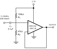
Typical Application

4 Revision History
Changes from B Revision (May 2013) to C Revision
- Added Device Information and Pin Configuration and Functions sections, ESD Ratings and Thermal Information tables, Functional Block Diagram, Feature Description, Device Functional Modes, Application and Implementation, Power Supply Recommendations, Layout, Device and Documentation Support, and Mechanical, Packaging, and Orderable Information sectionsGo
- Changed RθJA from 265°C/W to 182.7°C/WGo
Changes from A Revision (May 2013) to B Revision
- Changed layout of National Semiconductor data sheet to TI formatGo
5 Pin Configuration and Functions


Pin Functions
| PIN | I/O | DESCRIPTION | ||
|---|---|---|---|---|
| NAME | LMV116 | LMV118 | ||
| +IN | 3 | 3 | Input | Non-inverting input |
| –IN | 4 | 4 | Input | Inverting input |
| OUTPUT | 1 | 1 | Output | Output |
| SD | — | 5 | Input | Shutdown input. Active high, must be tied to V– with resistor for normal operation. |
| V+ | 5 | 6 | Power | Positive (highest) power supply |
| V– | 2 | 2 | Power | Negative (lowest) power supply |