SNOS018H August 1999 – December 2014 LMV331-N , LMV339-N , LMV393-N
PRODUCTION DATA.
- 1 Features
- 2 Applications
- 3 Description
- 4 Revision History
- 5 Pin Configuration and Functions
- 6 Specifications
- 7 Detailed Description
- 8 Application and Implementation
- 9 Power Supply Recommendations
- 10Layout
- 11Device and Documentation Support
- 12Mechanical, Packaging, and Orderable Information
Package Options
Mechanical Data (Package|Pins)
Thermal pad, mechanical data (Package|Pins)
Orderable Information
1 Features
- (For 5-V Supply, Typical Unless Otherwise Noted)
- Ensured 2.7-V and 5-V Performance
- Industrial Temperature Range −40°C to 85°C
- Low Supply Current 60 µA/Channel
- Input Common Mode Voltage Range Includes Ground
- Low Output Saturation Voltage 200 mV
- Propagation Delay 200 ns
- Space-Saving 5-Pin SC70 and 5-Pin SOT23 Packages
2 Applications
- Mobile Communications
- Notebooks and PDAs
- Battery-Powered Electronics
- General-Purpose Portable Devices
- General-Purpose, Low-Voltage Applications
3 Description
The LMV393-N and LMV339-N are low-voltage (2.7 to 5 V) versions of the dual and quad comparators, LM393/339, which are specified at 5 to 30 V. The LMV331-N is the single version, which is available in space-saving, 5-pin SC70 and 5-pin SOT23 packages. The 5-pin SC70 is approximately half the size of the 5-pin SOT23.
The LMV393-N is available in 8-pin SOIC and VSSOP packages. The LMV339-N is available in 14-pin SOIC and TSSOP packages.
The LMV331-N/393-N/339-N is the most cost-effective solution where space, low voltage, low power, and price are the primary specification in circuit design for portable consumer products. They offer specifications that meet or exceed the familiar LM393/339 at a fraction of the supply current.
The chips are built with TI's advanced Submicron Silicon-Gate BiCMOS process. The LMV331-N/393-N/339-N have bipolar input and output stages for improved noise performance.
Table 1. Device Information(1)
| PART NUMBER | PACKAGE | BODY SIZE (NOM) |
|---|---|---|
| LMV331-N | SC70 (5) | 2.00 mm × 1.25 mm |
| SOT-23 (5) | 2.90 mm × 1.6 mm | |
| LMV339-N | SOIC (14) | 8.65 mm × 3.91 mm |
| TSSOP (14) | 5.00 mm × 4.40 mm | |
| LMV393-N | SOIC (8) | 4.90 mm × 3.91 mm |
| VSSOP (8) | 3.00 mm × 3.00 mm |
- For all available packages, see the orderable addendum at the end of the datasheet.
Low Supply Current
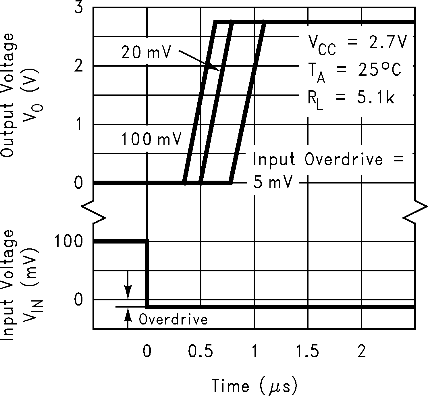
Fast Response Time