SNVS468L September   2006  â€“ November 2015 LP3972

PRODUCTION DATA.  

  1. Features
  2. Applications
  3. Description
  4. Revision History
  5. Device Comparison Tables
  6. Pin Configuration and Functions
  7. Specifications
    1. 7.1  Absolute Maximum Ratings
    2. 7.2  ESD Ratings
    3. 7.3  Recommended Operating Conditions
    4. 7.4  Thermal Information
    5. 7.5  Electrical Characteristics
    6. 7.6  Electrical Characteristics: LDO RTC
    7. 7.7  Electrical Characteristics: LDOs 1 to 5
    8. 7.8  Electrical Characteristics: Buck Converters SW1, SW2, SW3
    9. 7.9  Electrical Characteristics: Backup Charger
    10. 7.10 Electrical Characteristics: I2C Compatible Serial Interface (SDA and SCL)
    11. 7.11 Logic Inputs and Outputs DC Operating Conditions
    12. 7.12 I2C Compatible Serial Interface Timing Requirements (SDA and SCL)
    13. 7.13 Power-On Timing Delays
    14. 7.14 Typical Characteristics
      1. 7.14.1 LDO Dropout Voltage vs Load Current Collect Data for all LDOs
      2. 7.14.2 Buck1 Output Efficiency vs. Load Current Varied From 1 mA to 1.5 A
  8. Detailed Description
    1. 8.1 Overview
    2. 8.2 Functional Block Diagram
    3. 8.3 Feature Description
      1. 8.3.1 Buck Converter Operation
        1. 8.3.1.1 Circuit Operation
        2. 8.3.1.2 PWM Operation
          1. 8.3.1.2.1 Internal Synchronous Rectification
          2. 8.3.1.2.2 Current Limiting
        3. 8.3.1.3 PFM Operation
        4. 8.3.1.4 Soft Start
        5. 8.3.1.5 Low Dropout (LDO) Operation
        6. 8.3.1.6 Spread-Spectrum Feature
      2. 8.3.2 LP3972 Battery Switch Operation
    4. 8.4 Device Functional Modes
      1. 8.4.1 Start-Up Mode
      2. 8.4.2 Shutdown Mode
      3. 8.4.3 Standby Mode
      4. 8.4.4 Active Mode
    5. 8.5 Programming
      1. 8.5.1 LP3972 Reset Sequence
        1. 8.5.1.1 LP3972 Controls
          1. 8.5.1.1.1  Digital Interface Control Signals
          2. 8.5.1.1.2  Power Domain Enables
          3. 8.5.1.1.3  Power Domains Sequencing (Delay)
          4. 8.5.1.1.4  Power Supply Enable
          5. 8.5.1.1.5  Wake-up Functionality (PWR_ON, NTEST_JIG, SPARE and EXT_WAKEUP)
          6. 8.5.1.1.6  Internal Thermal Shutdown Procedure
          7. 8.5.1.1.7  Battery Switch and Backup Battery Charger
          8. 8.5.1.1.8  General Purpose I/O Functionality (GPIO1 And GPIO2)
          9. 8.5.1.1.9  Regulated Voltages OK
          10. 8.5.1.1.10 Thermal Management
          11. 8.5.1.1.11 Thermal Warning
          12. 8.5.1.1.12 LP3972 Thermal Flags Functional Diagram, Data from Initial Silicon
        2. 8.5.1.2 Initial Cold Start Power-On Sequence
        3. 8.5.1.3 Hardware Reset Sequence
        4. 8.5.1.4 Reset Sequence
      2. 8.5.2 I2C Compatible Interface
        1. 8.5.2.1 I2C Data Validity
        2. 8.5.2.2 I2C Start And Stop Conditions
        3. 8.5.2.3 Transferring Data
        4. 8.5.2.4 I2C Chip Address - 7h'34
          1. 8.5.2.4.1 Write Cycle
          2. 8.5.2.4.2 Read Cycle
        5. 8.5.2.5 Multi-Byte I2C Command Sequence
        6. 8.5.2.6 Incremental Register I2C Command Sequence
    6. 8.6 Register Maps
      1. 8.6.1 Serial Interface Register Selection Codes
        1. 8.6.1.1  System Control Status Register
          1. 8.6.1.1.1 System Control Register (SCR) 8h’07
          2. 8.6.1.1.2 System Control Register (SCR) 8h’07 Definitions
        2. 8.6.1.2  Output Voltage Enable Register 1
          1. 8.6.1.2.1 Output Voltage Enable Register 1 (OVER1) 8h’10
          2. 8.6.1.2.2 Output Voltage Enable Register 1 (OVER1) 8h’10 Definitions
        3. 8.6.1.3  Output Voltage Status Register
          1. 8.6.1.3.1 Output Voltage Status Register 1 (OVSR1) 8h’11
          2. 8.6.1.3.2 Output Voltage Status Register 1 (OVSR1) 8h’11 Definitions
        4. 8.6.1.4  Output Voltage Enable Register 2
          1. 8.6.1.4.1 Output Voltage Enable Register 2 (OVER2) 8h’12
          2. 8.6.1.4.2 Output Voltage Enable Register 2 (OVER2) 8h’12 Definitions
        5. 8.6.1.5  Output Voltage Status Register 2
          1. 8.6.1.5.1 Output Voltage Status Register 2 (OVSR2) 8h’13
          2. 8.6.1.5.2 Output Voltage Status Register 2 (OVSR2) 8h’13 Definitions
        6. 8.6.1.6  DVM Voltage Change Control Register 1
          1. 8.6.1.6.1 DVM Voltage Change Control Register 1 (VCC1) 8h’20
          2. 8.6.1.6.2 DVM Voltage Change Control Register 1 (VCC1) 8h’20 Definitions
        7. 8.6.1.7  Buck1 (VCC_APPS) Voltage 1
          1. 8.6.1.7.1 Buck1 (VCC_APPS) Target Voltage 1 Register (ADTV1) 8h’23
          2. 8.6.1.7.2 Buck1 (VCC_apps) Target Voltage 1 Register (ADTV1) 8h’23 Definitions
        8. 8.6.1.8  Buck1 (VCC_APPS) Target Voltage 2 Register
          1. 8.6.1.8.1 Buck1 (VCC_APPS) Target Voltage 2 Register (ADTV2) 8h’24
          2. 8.6.1.8.2 Buck1 (VCC_APPS) Target Voltage 2 Register (ADTV2) 8h’24 Definitions
        9. 8.6.1.9  Buck1 (VCC_APPS) Voltage Ramp Control Register
          1. 8.6.1.9.1 Buck1 (VCC_APPS) Voltage Ramp Control Register (AVRC) 8h’25
          2. 8.6.1.9.2 Buck1 (VCC_APPS) Voltage Ramp Control Register (AVRC) 8h’25 Definitions
        10. 8.6.1.10 VCC_comm Target Voltage 1 Dummy Register (CDTV1)
          1. 8.6.1.10.1 VCC_comm Target Voltage 1 Dummy Register (CDTV1) 8h’26 Write Only
        11. 8.6.1.11 VCC_COMM Target Voltage 2 Dummy Register (CDTV2)
          1. 8.6.1.11.1 VCC_COMM Target Voltage 2 Dummy Register (CDTV2) 8h’27 Write Only
        12. 8.6.1.12 LDO5 (VCC_SRAM) Target Voltage 1 Register
          1. 8.6.1.12.1 LDO5 (VCC_SRAM) Target Voltage 1 Register (SDTV1) 8h'29
          2. 8.6.1.12.2 LDO5 (VCC_SRAM) Target Voltage 1 Register (SDTV1) 8h’29 Definitions
        13. 8.6.1.13 LDO5 (VCC_SRAM) Target Voltage 2 Register
          1. 8.6.1.13.1 LDO5 (VCC_SRAM) Target Voltage 2 Register (SDTV2) 8h’2A
          2. 8.6.1.13.2 LDO5 (VCC_SRAM) Target Voltage 2 Register (SDTV2) 8h’2A Definitions
        14. 8.6.1.14 LDO1 (VCC_MVT) Target Voltage 1 Register (MDTV1)
          1. 8.6.1.14.1 LDO1 (VCC_MVT) Target Voltage 1 Register (MDTV1) 8h’32
          2. 8.6.1.14.2 LDO1 (VCC_MVT) Target Voltage 1 Register (MDTV1) 8h’32 Definitions
        15. 8.6.1.15 LDO1 (VCC_MVT) Target Voltage 2 Register
          1. 8.6.1.15.1 LDO1 (VCC_MVT) Target Voltage 2 Register (MDTV2) 8h’33
          2. 8.6.1.15.2 LDO1 (VCC_MVT) Target Voltage 2 Register (MDTV2) 8h’33 Definitions
        16. 8.6.1.16 LDO2 Voltage Control Register (L12VCR)
          1. 8.6.1.16.1 LDO2 Voltage Control Register (L12VCR) 8h’39
          2. 8.6.1.16.2 LDO2 Voltage Control Register (L12VCR) 8h’39 Definitions
        17. 8.6.1.17 LDO4 - LDO3 Voltage Control Register (L34VCR)
          1. 8.6.1.17.1 LDO4 - LDO3 Voltage Control Register (L34VCR) 8h’3A
          2. 8.6.1.17.2 LDO4 - LDO3 Voltage Control Register (L34VCR) 8h’3A Definitions
      2. 8.6.2 TI-Defined Control and Status Registers
        1. 8.6.2.1  System Control Register 1 (SCR1)
          1. 8.6.2.1.1 System Control Register 1 (SCR1) 8h’80
          2. 8.6.2.1.2 System Control Register 1 (SCR1) 8h’80 Definitions
        2. 8.6.2.2  System Control Register 2 (SCR2)
          1. 8.6.2.2.1 System Control Register 2 (SCR2) 8h’81
          2. 8.6.2.2.2 System Control Register 2 (SCR2) 8h’81 Definitions
        3. 8.6.2.3  Output Enable 3 Register (OEN3) 8h’82
        4. 8.6.2.4  Output Enable 3 Register (OEN3) 8h’82 Definitions
        5. 8.6.2.5  Status Register 3 (OSR3) 8h’83
        6. 8.6.2.6  Status Register 3 (OSR3) Definitions 8h’83
        7. 8.6.2.7  Logic Output Enable Register (LOER) 8h’84
        8. 8.6.2.8  Logic Output Enable Register (LOER) Definitions 8h’84
        9. 8.6.2.9  VCC_BUCK2 Target Voltage Register (B2TV) 8h’85
        10. 8.6.2.10 VCC_BUCK2 Target Voltage Register (B2TV) 8h’85 Definitions
        11. 8.6.2.11 BUCK3 Target Voltage Register (B3TV) 8h’86
        12. 8.6.2.12 BUCK3 Target Voltage Register (B3TV) 8h’86 Definitions
        13. 8.6.2.13 VCC_BUCK3:2 Voltage Ramp Control Register (B32RC)
          1. 8.6.2.13.1 VCC_BUCK3:2 Voltage Ramp Control Register (B32RC) 8h’87
          2. 8.6.2.13.2 Buck3:2 Voltage Ramp Control Register (B3RC) 8h’87 Definitions
        14. 8.6.2.14 Interrupt Status Register ISRA
          1. 8.6.2.14.1 Interrupt Status Register ISRA 8h’88
          2. 8.6.2.14.2 Interrupt Status Register ISRA 8h’88 Definitions
        15. 8.6.2.15 Backup Battery Charger Control Register (BCCR)
          1. 8.6.2.15.1 Backup Battery Charger Control Register (BCCR) 8h’89
          2. 8.6.2.15.2 Backup Battery Charger Control Register (BCCR) 8h’89 Definitions
        16. 8.6.2.16 Marvell PXA Internal 1 Revision Register (II1RR) 8h’8E
        17. 8.6.2.17 Marvell PXA Internal 1 Revision Register (II1RR) (Ii1rr) 8h’8E Definitions
        18. 8.6.2.18 Marvell PXA Internal 2 Revision Register (II1RR) 8h’8F
        19. 8.6.2.19 Marvell PXA Internal 2 Revision Register (II1RR) 8h’8F Definitions
        20. 8.6.2.20 Register Programming Examples
          1. 8.6.2.20.1 Example 1: Start-of-Day (SOD) Sequence
          2. 8.6.2.20.2 Example 2: Voltage Change Sequence
          3. 8.6.2.20.3 I2C Data Exchange Between Master and Slave Device
  9. Application and Implementation
    1. 9.1 Application Information
    2. 9.2 Typical Application
      1. 9.2.1 Design Requirements
      2. 9.2.2 Detailed Design Procedure
        1. 9.2.2.1 LDO Considerations
          1. 9.2.2.1.1 External Capacitors
          2. 9.2.2.1.2 Input Capacitor
          3. 9.2.2.1.3 Output Capacitor
          4. 9.2.2.1.4 No-Load Stability
          5. 9.2.2.1.5 Capacitor Characteristics
        2. 9.2.2.2 Buck Considerations
          1. 9.2.2.2.1 Inductor Selection
            1. 9.2.2.2.1.1 Method 1
            2. 9.2.2.2.1.2 Method 2
          2. 9.2.2.2.2 Input Capacitor Selection
          3. 9.2.2.2.3 Output Capacitor Selection
          4. 9.2.2.2.4 Buck Output Ripple Management
      3. 9.2.3 Application Curves
  10. 10Power Supply Recommendations
  11. 11Layout
    1. 11.1 Layout Guidelines
    2. 11.2 Layout Example
  12. 12Device and Documentation Support
    1. 12.1 Device Support
      1. 12.1.1 Third-Party Products Disclaimer
    2. 12.2 Related Documentation
    3. 12.3 Community Resources
    4. 12.4 Trademarks
    5. 12.5 Electrostatic Discharge Caution
    6. 12.6 Glossary
  13. 13Mechanical, Packaging, and Orderable Information

Package Options

Mechanical Data (Package|Pins)
Thermal pad, mechanical data (Package|Pins)
Orderable Information

1 Features

  • Compatible With Advanced Applications Processors Requiring Dynamic Voltage Management (DVM)
  • Backup Battery Charger With Automatic Switch for Lithium-Manganese Coin-Cell Batteries and Super Capacitors
  • I2C-Compatible High-Speed Serial Interface
  • Software Control of Regulator Functions and Settings
  • Thermal and Current Overload Protections
  • Three Buck Regulators for Powering High-Current Processor Functions or I/Os
    • Programmable VOUT from 0.725 V to 3.3 V
    • Up to 95% Efficiency and 1.6-A Output Current
    • ±3% Output Voltage Accuracy
  • Six LDOs for Powering RTC, Peripherals, and I/Os
    • Programmable VOUT of 1 V to 3.3 V
    • ±3% Output Voltage Accuracy
      • LDO_RTC 30 mA
      • LDO1 300 mA
      • LDO2 150 mA
      • LDO3 150 mA
      • LDO4 150 mA
      • LDO5 400 mA

2 Applications

  • Smart Phones
  • Personal Media Players
  • Digital Cameras
  • Application Processors
    • Marvell PXA
    • Freescale
    • Samsung

3 Description

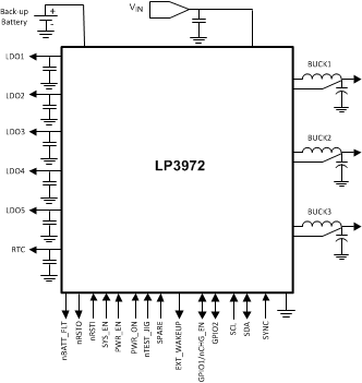
The LP3972 is a multi-function programmable power management unit (PMU) designed especially for advanced application processors. The LP3972 is optimized for low-power handheld applications and provides six low-dropout low-noise linear regulators, three DC-DC magnetic buck regulators, a backup battery charger, and two GPIOs. A high-speed serial interface is included to program individual regulator output voltages as well as on and off control.

Device Information(1)

PART NUMBER PACKAGE BODY SIZE (NOM)
LP3972 WQFN (40) 5.00 mm × 5.00 mm
  1. For all available packages, see the orderable addendum at the end of the data sheet.

Simplified Schematic

LP3972 20207601.gif