SNVSA66A October 2014 – December 2015 LP3990-Q1
PRODUCTION DATA.
- 1 Features
- 2 Applications
- 3 Description
- 4 Revision History
- 5 Pin Configuration and Functions
- 6 Specifications
- 7 Detailed Description
- 8 Application and Implementation
- 9 Power Supply Recommendations
- 10Layout
- 11Device and Documentation Support
- 12Mechanical, Packaging, and Orderable Information
Package Options
Mechanical Data (Package|Pins)
- YZR|4
Thermal pad, mechanical data (Package|Pins)
Orderable Information
1 Features
- Qualified for Automotive Applications
- AEC-Q100 Qualified With the Following Results
- Device Temperature Grade 1: –40°C to +125°C Ambient Operating Temperature Range
- Input Voltage Range: 2 V to 6 V
- 1% Voltage Accuracy at Room Temperature
- Output Voltage Range: 0.8 V to 3.3 V
- Output Current: 150 mA
- Logic Controlled Enable
- Thermal-Overload and Short-Circuit Protection
- Virtually Zero IQ (Disabled), < 10 nA
- Very Low IQ (Enabled): 43 µA
- Low Output Noise: 150 µVRMS
- PSRR: 55 dB at 1 kHz
- Fast Start-Up: 105 µs
- Stable with Ceramic Capacitor
- Output Stable - Capacitors, 1 µF
- No Noise Bypass Capacitor Required
2 Applications
- Infotainment
- Instrumentation
- Body Electronics
3 Description
The LP3990-Q1 regulator is designed to meet the requirements of portable, battery-powered systems providing an accurate output voltage, low-noise, and low-quiescent current. The LP3990-Q1 will provide a 0.8-V output from the low input voltage of 2 V at up to a 150-mA load current. When switched into shutdown mode via a logic signal at the enable pin (EN), the power consumption is reduced to virtually zero.
The LP3990-Q1 is designed to be stable with space-saving ceramic capacitors with values as low as 1 µF.
Performance is specified for a –40°C to +125°C junction temperature range.
For output voltage options please refer to package option addendum (POA) or contact the Texas Instruments Sales Office.
Device Information(1)
| PART NUMBER | PACKAGE | BODY SIZE |
|---|---|---|
| LP3990-Q1 | DSBGA (4) | 1.324 mm x 1.045 mm (MAX) |
- For all available packages, see the orderable addendum at the end of the data sheet.
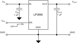
Simplified Schematic
