-
LPV511 Micropower, Rail-to-Rail Input and Output Operational Amplifier
- 1 Features
- 2 Applications
- 3 Description
- 4 Revision History
- 5 Pin Configuration and Functions
- 6 Specifications
- 7 Detailed Description
- 8 Application and Implementation
- 9 Power Supply Recommendations
- 10Layout
- 11Device and Documentation Support
- 12Mechanical, Packaging, and Orderable Information
- IMPORTANT NOTICE
Package Options
Mechanical Data (Package|Pins)
- DCK|5
Thermal pad, mechanical data (Package|Pins)
Orderable Information
LPV511 Micropower, Rail-to-Rail Input and Output Operational Amplifier
1 Features
- Wide Supply Voltage Range: 2.7 V to 12 V
- Slew Rate: 7.7 V/ms
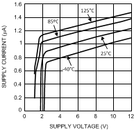
- Supply Current: 880 nA
- Output Short-Circuit Current: 1.35 mA
- Rail-to-Rail Input
- Rail-to-Rail Output: 100 mV from Rails
- Bandwidth (CL = 50 pF, RL = 1 MΩ): 27 kHz
- Unity Gain Stable
2 Applications
- Battery Powered Systems
- Security Systems
- Micropower Thermostats
- Solar Powered Systems
- Portable Instrumentation
- Micropower Filters
- Remote Sensor Amplifiers
3 Description
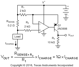
The LPV511 is a micropower operational amplifier that operates from a voltage supply range as wide as 2.7 V to 12 V with ensured specifications at 3 V, 5 V, and 12 V. The ultra-low power LPV511 exhibits an excellent speed to power ratio, drawing only 880 nA of supply current with a bandwidth of 27 kHz. These specifications make the LPV511 an ideal choice for battery-powered systems that require long life through low supply current, such as instrumentation, sensor conditioning and battery current monitoring.
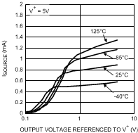
The LPV511 has an input range that includes both supply rails for ground and high-side battery sensing applications. The LPV511 output swings within 100 mV of either rail to maximize the signal's dynamic range in low supply applications. In addition, the output is capable of sourcing 650 µA of current when powered by a 12-V battery.
The LPV511 is fabricated on TI's advanced VIP50C process.
The LPV511 is available in the space-saving SC70 package, which makes it ideal for portable electronics with area-constrained PC boards.
Device Information(1)
| PART NUMBER | PACKAGE | BODY SIZE (NOM) |
|---|---|---|
| LPV511 | SC70 (5) | 2.00 mm × 1.25 mm |
- For all available packages, see the orderable addendum at the end of the data sheet.
Typical Supply Current
High-Side Battery Current Sensor
4 Revision History
Changes from C Revision (March 2013) to D Revision
- Added ESD Ratings table, Feature Description section, Device Functional Modes, Application and Implementation section, Power Supply Recommendations section, Layout section, Device and Documentation Support section, and Mechanical, Packaging, and Orderable Information section Go
- Added Thermal Information table Go
Changes from B Revision (March 2013) to C Revision
- Changed layout of National Semiconductor Data Sheet to TI formatGo
5 Pin Configuration and Functions

Pin Functions
| PIN | I/O | DESCRIPTION | |
|---|---|---|---|
| NO. | NAME | ||
| 1 | VOUT | O | Output |
| 2 | V– | P | Negative supply voltage |
| 3 | VIN+ | I | Noninverting input |
| 4 | VIN– | I | Inverting input |
| 5 | V+ | P | Positive supply voltage |
6 Specifications
6.1 Absolute Maximum Ratings
over operating free-air temperature range (unless otherwise noted)(1)(2)| MIN | MAX | UNIT | ||
|---|---|---|---|---|
| VIN Differential | 2.1 | V | ||
| Supply voltage (V+ - V−) | 13.2 | V | ||
| Voltage at input and output pins | V+ + 0.3 | V− − 0.3 | V | |
| Short-circuit duration | See(3) | |||
| Junction temperature, TJ(4) | 150 | °C | ||
| Storage temperature, Tstg | –65 | 150 | °C | |
6.2 ESD Ratings
| VALUE | UNIT | |||
|---|---|---|---|---|
| V(ESD) | Electrostatic discharge | Human-body model (HBM), per ANSI/ESDA/JEDEC JS-001(1)(2) | ±2000 | V |
| Machine model (MM)(3) | ±200 | |||
6.3 Recommended Operating Conditions
over operating free-air temperature range (unless otherwise noted)| MIN | MAX | UNIT | ||
|---|---|---|---|---|
| Temperature(1) | –40 | 85 | °C | |
| Supply voltage (V+ – V−) | 2.7 | 12 | V | |
6.4 Thermal Information
| THERMAL METRIC(1) | LPV511 | UNIT | |
|---|---|---|---|
| DCK (SC70) | |||
| 5 PINS | |||
| RθJA | Junction-to-ambient thermal resistance | 278 | °C/W |
| RθJC(top) | Junction-to-case (top) thermal resistance | 105.8 | °C/W |
| RθJB | Junction-to-board thermal resistance | 56.4 | °C/W |
| ψJT | Junction-to-top characterization parameter | 3 | °C/W |
| ψJB | Junction-to-board characterization parameter | 55 | °C/W |
| RθJC(bot) | Junction-to-case (bottom) thermal resistance | n/a | °C/W |
6.5 Electrical Characteristics: 3 V
Unless otherwise specified, all limits are specified for TJ = 25°C, V+ = 3 V, V− = 0 V, VCM = VO = V+/2, and RL = 100 kΩ to V+/2.(1)| PARAMETER | TEST CONDITIONS | MIN(2) | TYP(3) | MAX(2) | UNIT | ||
|---|---|---|---|---|---|---|---|
| VOS | Input offset voltage | TJ = 25°C | ±0.2 | ±3 | mV | ||
| TJ = –40°C to 85°C | ±3.8 | ||||||
| TC VOS | Input offset voltage drift(4) | TJ = 25°C | ±0.3 | µV/°C | |||
| TJ = –40°C to 85°C | ±15 | ||||||
| IB | Input bias current(5) | VCM = 0.5 V | TJ = 25°C | –1000 | –320 | pA | |
| TJ = –40°C to 85°C | –1600 | ||||||
| VCM = 2.5 V | TJ = 25°C | 110 | 800 | ||||
| TJ = –40°C to 85°C | 1900 | ||||||
| IOS | Input offset current | ±10 | pA | ||||
| CMRR | Common mode rejection ratio | VCM Stepped from 0 V to 1.5 V | TJ = 25°C | 77 | 100 | dB | |
| TJ = –40°C to 85°C | 70 | ||||||
| VCM Stepped from 2.4 V to 3 V | TJ = 25°C | 75 | 115 | ||||
| TJ = –40°C to 85°C | 68 | ||||||
| VCM Stepped from 0.5 V to 2.5 V | TJ = 25°C | 60 | 80 | ||||
| TJ = –40°C to 85°C | 56 | ||||||
| PSRR | Power supply rejection ratio | V+ = 2.7 V to 5 V, VCM = 0.5 V |
TJ = 25°C | 72 | 114 | dB | |
| TJ = –40°C to 85°C | 68 | ||||||
| V+ = 3 V to 5 V, VCM = 0.5 V |
TJ = 25°C | 76 | 115 | ||||
| TJ = –40°C to 85°C | 72 | ||||||
| V+ = 5 V to 12 V, VCM = 0.5 V |
TJ = 25°C | 84 | 117 | ||||
| TJ = –40°C to 85°C | 80 | ||||||
| CMVR | Input common-mode voltage | CMRR ≥ 50 dB | TJ = 25°C | −0.1 | 3.1 | V | |
| TJ = –40°C to 85°C | 0 | 3 | |||||
| AVOL | Large signal voltage gain | Sinking, VO = 2.5 V | TJ = 25°C | 75 | 105 | dB | |
| TJ = –40°C to 85°C | 70 | ||||||
| Sourcing, VO = 0.5 V | TJ = 25°C | 75 | 105 | ||||
| TJ = –40°C to 85°C | 70 | ||||||
| VO | Output swing high | VID = 100 mV | TJ = 25°C | 2.85 | 2.9 | V | |
| TJ = –40°C to 85°C | 2.8 | ||||||
| Output swing low | VID = −100 mV | TJ = 25°C | 100 | 150 | |||
| TJ = –40°C to 85°C | 200 | ||||||
| ISC | Output short circuit current(6) | Sourcing VID = 100 mV |
−500 | −225 | µA | ||
| Sinking VID = −100 mV |
225 | 1350 | |||||
| IS | Supply current | TJ = 25°C | 0.88 | 1.2 | µA | ||
| TJ = –40°C to 85°C | 1.5 | ||||||
| SR | Slew rate(7) | AV = 1, VO ramps from 0.5 V to 2.5 V | TJ = 25°C | 5.25 | 7.7 | V/ms | |
| TJ = –40°C to 85°C | 3.10 | ||||||
| GBW | Gain bandwidth product | RL = 1 MΩ, CL= 50 pF | 27 | kHz | |||
| Phase margin | RL = 1 MΩ, CL= 50 pF | 53 | º | ||||
| en | Input-referred voltage noise | f = 100 Hz | 320 | nV/√Hz | |||
| in | Input-referred current noise | f = 10 Hz | 0.02 | pA/√Hz | |||
| f = 1 kHz | 0.01 | ||||||
6.6 Electrical Characteristics: 5 V
Unless otherwise specified, all limits are specified for TJ = 25°C, V+ = 5 V, V− = 0 V, VCM = VO = V+/2, and RL = 100 kΩ to V+/2.(1)| PARAMETER | TEST CONDITIONS | MIN(2) | TYP(3) | MAX(2) | UNIT | ||
|---|---|---|---|---|---|---|---|
| VOS | Input offset voltage | TJ = 25°C | ±0.2 | ±3 | mV | ||
| TJ = –40°C to 85°C | ±3.8 | ||||||
| TC VOS | Input offset voltage drift(4) | TJ = 25°C | ±0.3 | µV/°C | |||
| TJ = –40°C to 85°C | ±15 | ||||||
| IB | Input bias current(5) | VCM = 0.5 V | TJ = 25°C | –1000 | –320 | pA | |
| TJ = –40°C to 85°C | –1600 | ||||||
| VCM = 4.5 V | TJ = 25°C | 110 | 800 | ||||
| TJ = –40°C to 85°C | 1900 | ||||||
| IOS | Input offset current | ±10 | pA | ||||
| CMRR | Common mode rejection ratio | VCM Stepped from 0 V to 2.5 V |
TJ = 25°C | 80 | 115 | dB | |
| TJ = –40°C to 85°C | 73 | ||||||
| VCM Stepped from 4.4 to 5 V |
TJ = 25°C | 75 | 107 | ||||
| TJ = –40°C to 85°C | 68 | ||||||
| VCM Stepped from 0.5 to 4.5 V |
TJ = 25°C | 65 | 87 | ||||
| TJ = –40°C to 85°C | 62 | ||||||
| PSRR | Power supply rejection ratio | V+ = 2.7 V to 5 V, VCM = 0.5 V |
TJ = 25°C | 72 | 114 | dB | |
| TJ = –40°C to 85°C | 68 | ||||||
| V+ = 3 V to 5 V, VCM = 0.5 V |
TJ = 25°C | 76 | 115 | ||||
| TJ = –40°C to 85°C | 72 | ||||||
| V+ = 5 V to 12 V, VCM = 0.5 V |
TJ = 25°C | 84 | 117 | ||||
| TJ = –40°C to 85°C | 80 | ||||||
| CMVR | Input common-mode voltage | CMRR ≥ 50 dB | TJ = 25°C | —0.1 | 5.1 | V | |
| TJ = –40°C to 85°C | 0 | 5 | |||||
| AVOL | Large signal voltage gain | Sinking, VO = 4.5 V | TJ = 25°C | 78 | 110 | dB | |
| TJ = –40°C to 85°C | 73 | ||||||
| Sourcing, VO = 0.5 V | TJ = 25°C | 78 | 110 | ||||
| TJ = –40°C to 85°C | 73 | ||||||
| VO | Output swing high | VID = 100 mV | TJ = 25°C | 4.8 | 4.89 | V | |
| TJ = –40°C to 85°C | 4.75 | ||||||
| Output swing low | VID = −100 mV | TJ = 25°C | 110 | 200 | mV | ||
| TJ = –40°C to 85°C | 250 | ||||||
| ISC | Output short circuit current(6) | Sourcing to V−
VID = 100 mV |
–550 | –225 | µA | ||
| Sinking to V+
VID = −100 mV |
225 | 1350 | |||||
| IS | Supply current | TJ = 25°C | 0.97 | 1.2 | µA | ||
| TJ = –40°C to 85°C | 1.5 | ||||||
| SR | Slew rate(7) | AV = 1, VO ramps from 0.5 V to 4.5 V |
TJ = 25°C | 5.25 | 7.5 | V/ms | |
| TJ = –40°C to 85°C | 3.1 | ||||||
| GBW | Gain bandwidth product | RL = 1 MΩ, CL= 50 pF | 27 | kHz | |||
| Phase margin | RL = 1 MΩ, CL= 50 pF | 53 | ° | ||||
| en | Input-referred voltage noise | f = 100 Hz | 320 | nV/√Hz | |||
| in | Input-referred current noise | f = 10 Hz | 0.02 | pA/√Hz | |||
| f = 1 kHz | 0.01 | ||||||
6.7 Electrical Characteristics: 12 V
Unless otherwise specified, all limits are specified for TJ = 25°C, V+ = 12 V, V− = 0 V, VCM = VO = V+/2, and RL = 100 kΩ to V+/2.(1)| PARAMETER | TEST CONDITIONS | MIN(2) | TYP (3) | MAX (2) | UNIT | ||
|---|---|---|---|---|---|---|---|
| VOS | Input offset voltage | TJ = 25°C | ±0.2 | ±3 | mV | ||
| TJ = –40°C to 85°C | ±3.8 | ||||||
| TC VOS | Input offset voltage drift(4) | TJ = 25°C | ±0.3 | µV/°C | |||
| TJ = –40°C to 85°C | ±15 | ||||||
| IB | Input bias current(5) | VCM = 0.5 V | TJ = 25°C | −1000 | −320 | pA | |
| TJ = –40°C to 85°C | −1600 | ||||||
| VCM = 11.5 V | TJ = 25°C | 110 | 800 | ||||
| TJ = –40°C to 85°C | 1900 | ||||||
| IOS | Input offset current | ±10 | pA | ||||
| CMRR | Common mode rejection ratio | VCM Stepped from 0 V to 6 V |
TJ = 25°C | 75 | 115 | dB | |
| TJ = –40°C to 85°C | 70 | ||||||
| VCM Stepped from 11.4 V to 12 V |
TJ = 25°C | 75 | 110 | ||||
| TJ = –40°C to 85°C | 68 | ||||||
| VCM Stepped from 0.5 V to 11.5 V |
TJ = 25°C | 70 | 97 | ||||
| TJ = –40°C to 85°C | 65 | ||||||
| PSRR | Power supply rejection ratio | V+ = 2.7 V to 5 V, VCM = 0.5 V |
TJ = 25°C | 72 | 114 | ||
| TJ = –40°C to 85°C | 68 | ||||||
| V+ = 3 V to 5 V, VCM = 0.5 V |
TJ = 25°C | 76 | 115 | ||||
| TJ = –40°C to 85°C | 72 | ||||||
| V+ = 5 V to 12 V, VCM = 0.5 V |
TJ = 25°C | 84 | 117 | ||||
| TJ = –40°C to 85°C | 80 | ||||||
| CMVR | Input common-mode voltage | CMRR ≥ 50 dB | TJ = 25°C | −0.1 | 12.1 | V | |
| TJ = –40°C to 85°C | 0 | 12 | |||||
| AVOL | Large signal voltage gain | Sinking, VO = 0.5 V | TJ = 25°C | 89 | 110 | dB | |
| TJ = –40°C to 85°C | 84 | ||||||
| Sourcing, VO = 11.5 V | TJ = 25°C | 89 | 110 | ||||
| TJ = –40°C to 85°C | 84 | ||||||
| VO | Output swing high | VID = 100 mV | TJ = 25°C | 11.8 | 11.85 | V | |
| TJ = –40°C to 85°C | 11.72 | ||||||
| Output swing low | VID = −100 mV | TJ = 25°C | 150 | 200 | mV | ||
| TJ = –40°C to 85°C | 280 | ||||||
| ISC | Output short circuit current(6) | Sourcing VID = 100 mV |
−650 | −200 | µA | ||
| Sinking VID = −100 mV |
200 | 1300 | |||||
| IS | Supply current | TJ = 25°C | 1.2 | 1.75 | µA | ||
| TJ = –40°C to 85°C | 2.5 | ||||||
| SR | Slew rate(7) | AV = 1, VO ramped from 1 V to 11 V | 5.25 | 7 | V/ms | ||
| 3.1 | |||||||
| GBW | Gain bandwidth product | RL = 1 MΩ, CL= 50 pF | 25 | kHz | |||
| Phase margin | RL = 1 MΩ, CL= 50 pF | 52 | ° | ||||
| en | Input-referred voltage noise | f = 100 Hz | 320 | nV/√Hz | |||
| in | Input-referred current noise | f = 10 Hz | 0.02 | pA/√Hz | |||
| f = 1 kHz | 0.01 | ||||||
6.8 Typical Characteristics
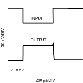
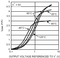
At TJ = 25°C, unless otherwise specified.
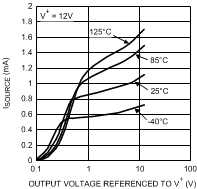
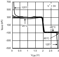
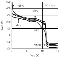

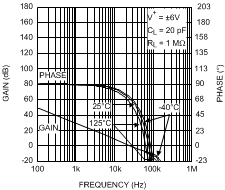
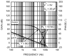
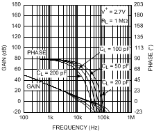
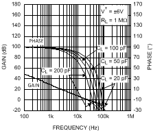
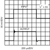
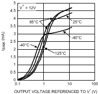
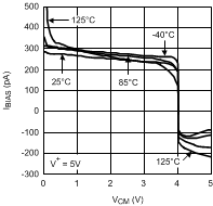
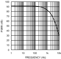
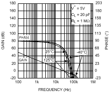
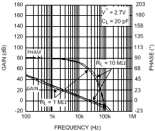
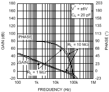
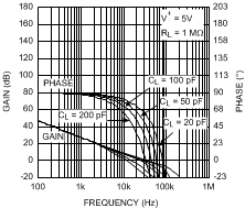
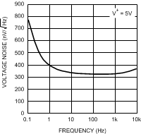
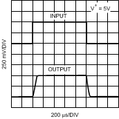
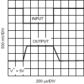
7 Detailed Description
7.1 Overview
The LPV511 is a micropower operational amplifier that operates from a voltage supply range as wide as 2.7 V to 12 V with ensured specifications at 3 V, 5 V, and 12 V. The LPV511 exhibits an excellent speed-to-power ratio, drawing only 880 nA of supply current with a bandwidth of 27 kHz.
7.2 Functional Block Diagram
7.3 Feature Description
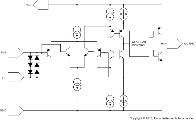
The LPV511 has a rail-to-rail input which provides more flexibility for the system designer. As can be seen from Functional Block Diagram, rail-to-rail input is achieved by using in parallel, one PNP differential pair and one NPN differential pair. When the common mode input voltage (VCM) is near V+, the NPN pair is on and the PNP pair is off. When VCM is near V−, the NPN pair is off and the PNP pair is on. When VCM is between V+ and V−, internal logic decides how much current each differential pair will get. This special logic ensures stable and low distortion amplifier operation within the entire common mode voltage range.
7.4 Device Functional Modes
7.4.1 Input Stage
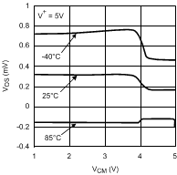
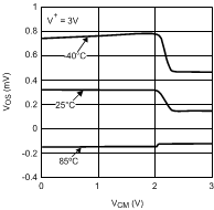
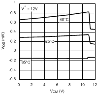
Because both input stages have their own offset voltage (VOS) characteristic, the offset voltage of the LPV511 becomes a function of VCM. VOS has a crossover point at 1 V below V+. See the VOS vs VCM curve in Typical Characteristics. Caution must be taken in situations where the input signal amplitude is comparable to the VOS value and/or the design requires high accuracy. In these situations, it is necessary for the input signal to avoid the crossover point.
The input bias current, IB will change in value and polarity as the input crosses the transition region. In addition, parameters such as PSRR and CMRR which involve the input offset voltage will also be affected by changes in VCM across the differential pair transition region.
Differential input voltage is the difference in voltage between the noninverting (+) input and the inverting input (−) of the op amp. Due to the three series diodes across the two inputs, the absolute maximum differential input voltage is ±2.1 V. This may not be a problem to most conventional op amp designs; however, designers must avoid using the LPV511 as a comparator.
7.4.2 Output Stage
The LPV511 output voltage swing 100 mV from rails at 3-V supply, which provides the maximum possible dynamic range at the output. This is particularly important when operating on low supply voltages.
The LPV511 maximum output voltage swing defines the maximum swing possible under a particular output load. The LPV511 output swings 110 mV from the rail at 5-V supply with an output load of 100 kΩ.
7.4.3 Driving Capacitive Load
The LPV511 is internally compensated for stable unity gain operation, with a 27-kHz typical gain bandwidth. However, the unity gain follower is the most sensitive configuration to capacitive load. Direct capacitive loading reduces the phase margin of the op amp. When the output is required to drive a large capacitive load, greater than 100 pF, a small series resistor at the output of the amplifier improves the phase margin (see Figure 27).
In Figure 27, the isolation resistor RISO and the load capacitor CL form a pole to increase stability by adding more phase margin to the overall system. The desired performance depends on the value of RISO. The bigger the RISO resistor value, the more stable VOUT will be. But the DC accuracy is degraded when the RISO gets bigger. If there were a load resistor in Figure 27, the output voltage would be divided by RISO and the load resistor.
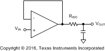 Figure 27. Resistive Isolation of Capacitive Load