-
OPA2171-EP 36-V, Single-Supply, SOT553, General-Purpose Operational Amplifiers
- 1 Features
- 2 Applications
- 3 Description
- 4 Revision History
- 5 Pin Configuration and Functions
- 6 Specifications
- 7 Detailed Description
- 8 Application and Implementation
- 9 Power Supply Recommendations
- 10Layout
- 11Device and Documentation Support
- 12Mechanical, Packaging, and Orderable Information
- IMPORTANT NOTICE
Package Options
Mechanical Data (Package|Pins)
- DCU|8
Thermal pad, mechanical data (Package|Pins)
Orderable Information
OPA2171-EP 36-V, Single-Supply, SOT553, General-Purpose Operational Amplifiers
1 Features
- Supply Range: 2.7 to 36 V, ±1.35 V to ±18 V
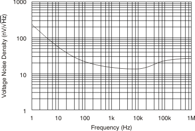
- Low Noise: 14 nV/√Hz
- Low Offset Drift: ±0.3 µV/°C (Typ)
- RFI Filtered Inputs
- Input Range Includes the Negative Supply
- Input Range Operates to Positive Supply
- Rail-to-Rail Output
- Gain Bandwidth: 3 MHz
- Low Quiescent Current: 475 µA per Amplifier
- High Common-Mode Rejection: 120 dB (Typ)
- Low-Input Bias Current: 8 pA
- microPackage: Dual in VSSOP-8
-
Supports Defense, Aerospace, and Medical Applications:
- Controlled Baseline
- One Assembly/Test Site
- One Fabrication Site
- Available in Extended (–55°C to 125°C) Temperature Range
- Extended Product Life Cycle
- Extended Product-Change Notification
- Product Traceability
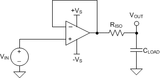
Unity-Gain Buffer With RISO Stability Compensation
2 Applications
- Tracking Amplifier in Power Modules
- Merchant Power Supplies
- Transducer Amplifiers
- Bridge Amplifiers
- Temperature Measurements
- Strain Gauge Amplifiers
- Precision Integrators
- Battery-Powered Instruments
- Test Equipment
3 Description
The OPA2171-EP is a 36-V, single-supply, low-noise operational amplifier with the ability to operate on supplies ranging from 2.7 V (±1.35 V) to 36 V (±18 V). These devices are available in micro-packages and offer low offset, drift, and bandwidth with low quiescent current. The single, dual, and quad versions all have identical specifications for maximum design flexibility.
Unlike most operational amplifiers, which are specified at only one supply voltage, the OPA2171-EP is specified from 2.7 to 36 V. Input signals beyond the supply rails do not cause phase reversal. The OPA2171-EP is stable with capacitive loads up to 300 pF. The input can operate 100 mV below the negative rail and within 2 V of the top rail during normal operation. Note that these devices can operate with full rail-to-rail input 100 mV beyond the top rail, but with reduced performance within 2 V of the top rail.
The OPA2171-EP operational amplifier is specified from –55°C to 125°C.
Device Information(1)
| PART NUMBER | PACKAGE | BODY SIZE (NOM) |
|---|---|---|
| OPA2171-EP | VSSOP (8) | 2.30 mm × 2.00 mm |
- For all available packages, see the orderable addendum at the end of the data sheet.
4 Revision History
| DATE | REVISION | NOTES |
|---|---|---|
| September 2015 | * | Initial release. |
5 Pin Configuration and Functions

Pin Functions
| PIN | I/O | DESCRIPTION | |
|---|---|---|---|
| NAME | NO. | ||
| +IN A | 3 | I | Noninverting input, channel A |
| +IN B | 5 | I | Noninverting input, channel B |
| –IN A | 2 | I | Inverting input, channel A |
| –IN B | 6 | I | Inverting input, channel B |
| OUT A | 1 | O | Output, channel A |
| OUT B | 7 | O | Output, channel B |
| V+ | 7 | — | Positive (highest) power supply |
| V– | 4 | — | Negative (lowest) power supply |
6 Specifications
6.1 Absolute Maximum Ratings
over operating free-air temperature range, unless otherwise noted(1)| MIN | MAX | UNIT | ||
|---|---|---|---|---|
| Supply voltage | ±20 | V | ||
| Signal input pins | Voltage | (V–) – 0.5 | (V+) + 0.5 | V |
| Current | –10 | 10 | mA | |
| Output short circuit(2) | Continuous | |||
| Junction temperature | 150 | °C | ||
| Storage temperature, Tstg | –65 | 150 | °C | |
6.2 ESD Ratings
| VALUE | UNIT | |||
|---|---|---|---|---|
| V(ESD) | Electrostatic discharge | Human-body model (HBM), per ANSI/ESDA/JEDEC JS-001(1) | ±4000 | V |
| Charged-device model (CDM), per JEDEC specification JESD22-C101(2) | ±750 | |||
6.3 Recommended Operating Conditions
over operating free-air temperature range (unless otherwise noted)| MIN | NOM | MAX | UNIT | ||
|---|---|---|---|---|---|
| Supply voltage (V+ – V–) | 4.5 (±2.25) | 36 (±18) | V | ||
| Operating temperature, TJ | –55 | 125 | °C | ||
6.4 Thermal Information
| THERMAL METRIC(1) | OPA2171-EP | UNIT | |
|---|---|---|---|
| DCU (VSSOP) | |||
| 8 PINS | |||
| RθJA | Junction-to-ambient thermal resistance | 175.2 | °C/W |
| RθJC(top) | Junction-to-case(top) thermal resistance | 74.9 | °C/W |
| RθJB | Junction-to-board thermal resistance | 22.2 | °C/W |
| ψJT | Junction-to-top characterization parameter | 1.6 | °C/W |
| ψJB | Junction-to-board characterization parameter | 22.8 | °C/W |
| RθJC(bot) | Junction-to-case(bottom) thermal resistance | N/A | °C/W |
6.5 Electrical Characteristics
at TJ = 25°C, VS = 2.7 to 36 V, VCM = VOUT = VS / 2, and RLOAD = 10 kΩ connected to VS / 2, unless otherwise noted.| PARAMETER | TEST CONDITIONS | MIN | TYP | MAX | UNIT | ||
|---|---|---|---|---|---|---|---|
| OFFSET VOLTAGE | |||||||
| Input offset voltage | VOS | 0.25 | ±1.8 | mV | |||
| Over temperature | TJ = –55°C to 125°C | 0.3 | ±2 | mV | |||
| Drift | dVOS/dT | TJ = –55°C to 125°C | 0.3 | µV/°C | |||
| vs power supply | PSRR | VS = 4 to 36 V, TA = –55°C to 125°C | 1 | ±5 | µV/V | ||
| Channel separation, dc | dc | 5 | µV/V | ||||
| INPUT BIAS CURRENT | |||||||
| Input bias current | IB | ±8 | ±15 | pA | |||
| Over temperature | TJ = –55°C to 125°C | ±4 | nA | ||||
| Input offset current | IOS | ±4 | pA | ||||
| Over temperature | TJ = –55°C to 125°C | ±4 | nA | ||||
| NOISE | |||||||
| Input voltage noise | ƒ = 0.1 to 10 Hz | 3 | µVPP | ||||
| Input voltage noise density | en | ƒ = 100 Hz | 25 | nV/√Hz | |||
| ƒ = 1 kHz | 14 | nV/√Hz | |||||
| INPUT VOLTAGE | |||||||
| Common-mode voltage range(1) | VCM | (V–) – 0.1 V | (V+) – 2 V | V | |||
| Common-mode rejection ratio | CMRR | VS = ±2 V, (V–) – 0.1 V < VCM < (V+) – 2 V, TJ = –55°C to 125°C |
87 | 104 | dB | ||
| VS = ±18 V, (V–) – 0.1 V < VCM < (V+) – 2 V, TJ = –55°C to 125°C |
104 | 120 | dB | ||||
| INPUT IMPEDANCE | |||||||
| Differential | 100 || 3 | MΩ || pF | |||||
| Common-mode | 6 || 3 | 1012Ω || pF | |||||
| OPEN-LOOP GAIN | |||||||
| Open-loop voltage gain | AOL | VS = 4 to 36 V, (V–) + 0.35 V < VO < (V+) – 0.35 V, TJ = –55°C to 125°C | 110 | 130 | dB | ||
| FREQUENCY RESPONSE | |||||||
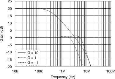
| Gain bandwidth product | GBP | 3.0 | MHz | ||||
| Slew rate | SR | G = +1 | 1.5 | V/µs | |||
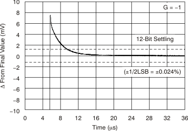
| Settling time | tS | To 0.1%, VS = ±18 V, G = +1, 10-V step | 6 | µs | |||
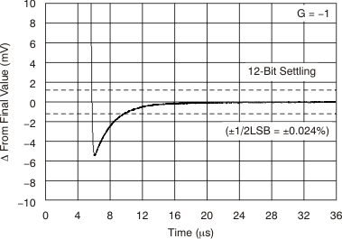
| To 0.01% (12 bit), VS = ±18 V, G = +1, 10-V step | 10 | µs | |||||
| Overload recovery time | VIN × Gain > VS | 2 | µs | ||||
| Total harmonic distortion + noise | THD+N | G = +1, ƒ = 1kHz, VO = 3VRMS | 0.0002% | ||||
| OUTPUT | |||||||
| Voltage output swing from rail | VO | VS = 5 V, RL = 10 kΩ | 30 | mV | |||
| Over temperature | RL = 10 kΩ, AOL ≥ 110 dB, TJ = –55°C to 125°C |
(V–) + 0.35 | (V+) – 0.35 | V | |||
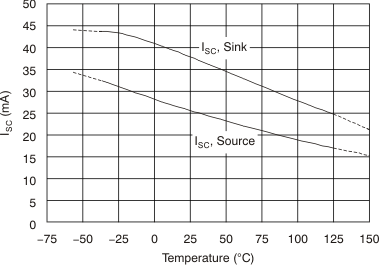
| Short-circuit current | ISC | +25/–35 | mA | ||||
| Capacitive load drive | CLOAD | See Typical Characteristics | pF | ||||
| Open-loop output resistance | RO | ƒ = 1 MHz, IO = 0 A | 150 | Ω | |||
| POWER SUPPLY | |||||||
| Specified voltage range | VS | 2.7 | 36 | V | |||
| Quiescent current per amplifier | IQ | IO = 0 A | 475 | 595 | µA | ||
| Over temperature | IO = 0 A, TJ = –55°C to 125°C | 650 | µA | ||||
| TEMPERATURE | |||||||
| Operating temperature | TJ | –55 | 125 | °C | |||
6.6 Typical Characteristics
Table 1. Characteristic Performance Measurements
| DESCRIPTION | FIGURE |
|---|---|
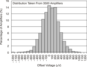
| Offset Voltage Production Distribution | Figure 1 |
| Offset Voltage Drift Distribution | Figure 2 |
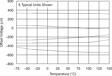
| Offset Voltage vs Temperature | Figure 3 |
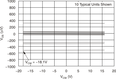
| Offset Voltage vs Common-Mode Voltage | Figure 4 |
| Offset Voltage vs Common-Mode Voltage (Upper Stage) | Figure 5 |
| Offset Voltage vs Power Supply | Figure 6 |
| IB and IOS vs Common-Mode Voltage | Figure 7 |
| Input Bias Current vs Temperature | Figure 8 |
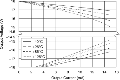
| Output Voltage Swing vs Output Current (Maximum Supply) | Figure 9 |
| CMRR and PSRR vs Frequency (Referred-to Input) | Figure 10 |
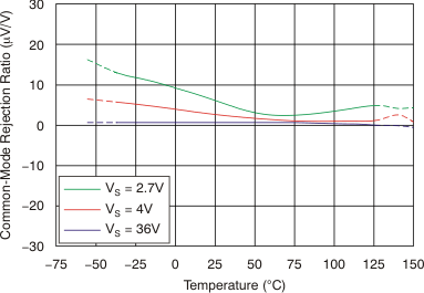
| CMRR vs Temperature | Figure 11 |
| PSRR vs Temperature | Figure 12 |
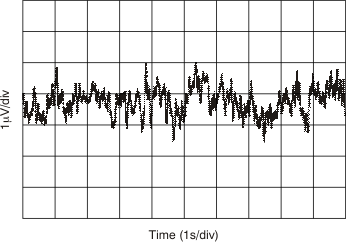
| 0.1-Hz to 10-Hz Noise | Figure 13 |
| Input Voltage Noise Spectral Density vs Frequency | Figure 14 |
| THD+N Ratio vs Frequency | Figure 15 |
| THD+N vs Output Amplitude | Figure 16 |
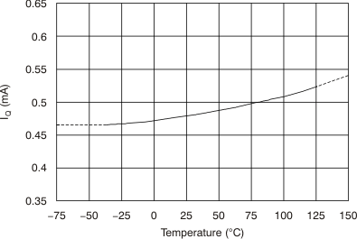
| Quiescent Current vs Temperature | Figure 17 |
| Quiescent Current vs Supply Voltage | Figure 18 |
| Open-Loop Gain and Phase vs Frequency | Figure 19 |
| Closed-Loop Gain vs Frequency | Figure 20 |
| Open-Loop Gain vs Temperature | Figure 21 |
| Open-Loop Output Impedance vs Frequency | Figure 22 |
| Small-Signal Overshoot vs Capacitive Load (100-mV Output Step) | Figure 23, Figure 24 |
| No Phase Reversal | Figure 25 |
| Positive Overload Recovery | Figure 26 |
| Negative Overload Recovery | Figure 27 |
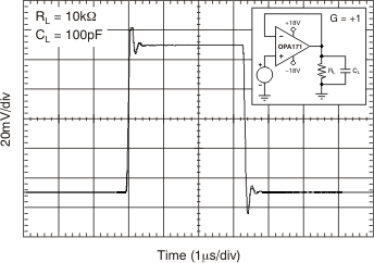
| Small-Signal Step Response (100 mV) | Figure 28, Figure 29 |
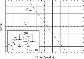
| Large-Signal Step Response | Figure 30, Figure 31 |
| Large-Signal Settling Time (10-V Positive Step) | Figure 32 |
| Large-Signal Settling Time (10-V Negative Step) | Figure 33 |
| Short-Circuit Current vs Temperature | Figure 34 |
| Maximum Output Voltage vs Frequency | Figure 35 |
| Channel Separation vs Frequency | Figure 36 |
