-
OPAx316-Q1 10-MHz, Rail-to-Rail Input/Output, Low-Voltage, 1.8-V CMOS Operational Amplifier SBOS841A November 2016 – January 2017 OPA2316-Q1 , OPA316-Q1 , OPA4316-Q1
PRODUCTION DATA.
-
OPAx316-Q1 10-MHz, Rail-to-Rail Input/Output, Low-Voltage, 1.8-V CMOS Operational Amplifier
- 1 Features
- 2 Applications
- 3 Description
- 4 Revision History
- 5 Pin Configuration and Functions
- 6 Specifications
- 7 Detailed Description
- 8 Application and Implementation
- 9 Power Supply Recommendations
- 10Layout
- 11Device and Documentation Support
- 12Mechanical, Packaging, and Orderable Information
- IMPORTANT NOTICE
Package Options
Mechanical Data (Package|Pins)
- DBV|5
Thermal pad, mechanical data (Package|Pins)
Orderable Information
OPAx316-Q1 10-MHz, Rail-to-Rail Input/Output, Low-Voltage, 1.8-V CMOS Operational Amplifier
1 Features
- Qualified for Automotive Applications
- AEC-Q100 Qualified With the Following Results:
- Unity-Gain Bandwidth: 10 MHz
- Low IQ: 400 µA/ch
- Wide Supply Range: 1.8 V to 5.5 V
- Low Noise: 11 nV/√Hz at 1 kHz
- Low Input Bias Current: ±5 pA
- Offset Voltage: ±0.5 mV
- Unity-Gain Stable
- Internal RFI-EMI Filter
- Extended Temperature Range: –40°C to +125°C
2 Applications
- Automotive Applications:
- ADAS
- Body Electronics and Lighting
- Current Sensing
- Battery Management Systems
3 Description
The OPAx316-Q1 family of single and dual operational amplifiers represents a new generation of general-purpose, low-power operational amplifiers. Featuring rail-to-rail input and output swings, low quiescent current (400 μA/ch typical) combined with a wide bandwidth of 10 MHz and very-low noise
(11 nV/√Hz at 1 kHz) makes this family suitable for circuits requiring a good speed and power ratio. The low input bias current supports those operational amplifiers for applications with megaohm source impedances. The low input bias current of the OPAx316-Q1 yields a very-low current noise to make the device attractive for high impedance sensor interfaces.
The robust design of the OPAx316-Q1 provides ease-of-use to the circuit designer: a unity-gain stable, integrated RFI and EMI rejection filter, no phase reversal in overdrive condition, and high electrostatic discharge (ESD) protection (4-kV HBM).
These devices are optimized for low-voltage operation as low as 1.8 V (±0.9 V) and up to 5.5 V (±2.75 V). This latest addition of low-voltage CMOS automotive grade operational amplifiers provide a family of wide bandwidth, low noise, and low power that meet the needs of a wide variety of applications.
Device Information(1)
| PART NUMBER | PACKAGE | BODY SIZE (NOM) |
|---|---|---|
| OPA316-Q1 | SOT-23 (5) | 1.60 mm × 2.90 mm |
| OPA2316-Q1 | VSSOP (8) | 3.00 mm × 3.00 mm |
| OPA4316-Q1 | TSSOP (14) | 4.40 mm × 5.00 mm |
- For all available packages, see the orderable addendum at the end of the data sheet.
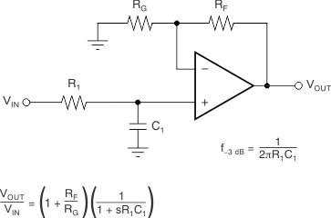
Single-Pole, Low-Pass Filter

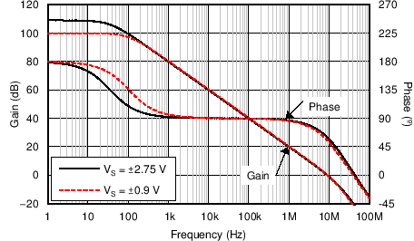
Low-Supply Current (400 µA/ch) for 10-MHz Bandwidth

4 Revision History
Changes from * Revision (November 2016) to A Revision
- Changed CDM classification reduced from C6 Go
- Deleted OPA2316S-Q1 package and body size information from Device Information table Go
- Deleted SC70 (5) (OPA316-Q1), DFN (8), MSOP (8), SOIC (8) (OPA2316-Q1), and SOIC (14) packages (OPA4316-Q1) from the Device Information table, Thermal Information tables, and pinout diagramsGo
- Deleted OPA2316S-Q1 pin diagram and Pin Functions table in Pin Configurations and Functions section Go
- Deleted D (SOIC) package from OPA4316-Q1 pin diagram in Pin Configurations and Functions section Go
- Changed CDM rating from ±1500 V to ±750 VGo
- Deleted OPA2316S-Q1 device thermal information in the Thermal Information table Go
- Added thermal information for OPA4316-Q1 deviceGo
- Deleted the literature numbers in parentheses from the format of TI document references in the Documentation Support section Go
5 Pin Configuration and Functions
Pin Functions: OPA316-Q1
| PIN | I/O | DESCRIPTION | |
|---|---|---|---|
| NAME | NO. | ||
| –IN | 4 | I | Inverting input |
| +IN | 3 | I | Noninverting input |
| V– | 2 | — | Negative supply or ground (for single-supply operation). |
| V+ | 5 | — | Positive supply |
| OUT | 1 | O | Output |
Pin Functions: OPA2316-Q1
| PIN | I/O | DESCRIPTION | |
|---|---|---|---|
| NAME | NO. | ||
| –IN A | 2 | I | Inverting input, channel A |
| +IN A | 3 | I | Noninverting input, channel A |
| –IN B | 6 | I | Inverting input, channel B |
| +IN B | 5 | I | Noninverting input, channel B |
| OUT A | 1 | O | Output, channel A |
| OUT B | 7 | O | Output, channel B |
| V– | 4 | — | Negative supply or ground (for single-supply operation). |
| V+ | 8 | — | Positive supply |
Pin Functions: OPA4316-Q1
| PIN | I/O | DESCRIPTION | |
|---|---|---|---|
| NAME | NO. | ||
| –IN A | 2 | I | Inverting input, channel A |
| +IN A | 3 | I | Noninverting input, channel A |
| –IN B | 6 | I | Inverting input, channel B |
| +IN B | 5 | I | Noninverting input, channel B |
| –IN C | 9 | I | Inverting input, channel C |
| +IN C | 10 | I | Noninverting input, channel C |
| –IN D | 13 | I | Inverting input, channel D |
| +IN D | 12 | I | Noninverting input, channel D |
| OUT A | 1 | O | Output, channel A |
| OUT B | 7 | O | Output, channel B |
| OUT C | 8 | O | Output, channel C |
| OUT D | 14 | O | Output, channel D |
| V– | 11 | — | Negative supply or ground (for single-supply operation) |
| V+ | 4 | — | Positive supply |