-
OPAx333 1.8-V, microPower, CMOS Operational Amplifiers, Zero-Drift Series
- 1 Features
- 2 Applications
- 3 Description
- 4 Revision History
- 5 Pin Configuration and Functions
- 6 Specifications
- 7 Detailed Description
- 8 Application and Implementation
- 9 Power Supply Recommendations
- 10Layout
- 11Device and Documentation Support
- 12Mechanical, Packaging, and Orderable Information
- IMPORTANT NOTICE
Package Options
Mechanical Data (Package|Pins)
Thermal pad, mechanical data (Package|Pins)
Orderable Information
OPAx333 1.8-V, microPower, CMOS Operational Amplifiers, Zero-Drift Series
1 Features
2 Applications
- Transducers
- Temperature Measurements
- Electronic Scales
- Medical Instrumentation
- Battery-Powered Instruments
- Handheld Test Equipment
3 Description
The OPAx333 series of CMOS operational amplifiers use a proprietary auto-calibration technique to simultaneously provide very low offset voltage (10 μV, maximum) and near-zero drift over time and temperature. These miniature, high-precision, low quiescent current amplifiers offer high-impedance inputs that have a common-mode range 100 mV beyond the rails, and rail-to-rail output that swings within 50 mV of the rails. Single or dual supplies as low as 1.8 V (±0.9 V) and up to 5.5 V (±2.75 V) can be used. These devices are optimized for low-voltage, single-supply operation.
The OPAx333 family offers excellent CMRR without the crossover associated with traditional complementary input stages. This design results in superior performance for driving analog-to-digital converters (ADCs) without degradation of differential linearity.
The OPA333 (single version) is available in the 5-pin SOT-23, SOT, and 8-pin SOIC packages, while the OPA2333 (dual version) is available in the 8-pin VSON, SOIC, and VSSOP packages. All versions are specified for operation from –40°C to 125°C.
Device Information(1)
| PART NUMBER | PACKAGE | BODY SIZE (NOM) |
|---|---|---|
| OPA333 | SOT-23 (5) | 2.90 mm × 1.60 mm |
| SOT (5) | 2.00 mm x 1.25 mm | |
| SOIC (8) | 4.90 mm × 3.90 mm | |
| OPA2333 | VSON (8) | 3.00 mm × 3.00 mm |
| SOIC (8) | 4.90 mm × 3.90 mm | |
| VSSOP (8) | 3.00 mm × 3.00 mm |
- For all available packages, see the orderable addendum at the end of the data sheet.
4 Revision History
Changes from D Revision (November 2013) to E Revision
- Added Pin Configuration and Functions section, ESD Ratings and Thermal Information tables, Feature Description section, Device Functional Modes, Application and Implementation section, Power Supply Recommendations section, Layout section, Device and Documentation Support section, and Mechanical, Packaging, and Orderable Information section Go
Changes from C Revision (May 2007) to D Revision
5 Pin Configuration and Functions


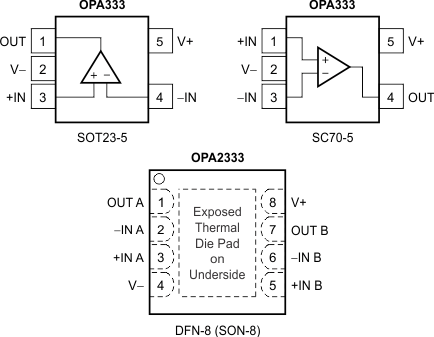
Pin Functions: OPA333
| PIN | I/O | DESCRIPTION | |||
|---|---|---|---|---|---|
| NAME | SOIC | SOT | SC70 | ||
| +IN | 3 | 3 | 1 | I | Noninverting input |
| –IN | 2 | 4 | 3 | I | Inverting input |
| NC | 1, 5, 8 | — | — | — | No internal connection (can be left floating) |
| OUT | 6 | 1 | 4 | O | Output |
| V+ | 7 | 5 | 5 | — | Positive (highest) power supply |
| V– | 4 | 2 | 2 | — | Negative (lowest) power supply |


Pin Functions: OPA2333
| PIN | I/O | DESCRIPTION | ||
|---|---|---|---|---|
| NAME | VSON | SOIC, VSSOP | ||
| +IN | — | — | I | Noninverting input |
| +IN A | 3 | 3 | I | Noninverting input, channel A |
| +IN B | 5 | 5 | I | Noninverting input, channel B |
| –IN | — | — | I | Inverting input |
| –IN A | 2 | 2 | I | Inverting input, channel A |
| –IN B | 6 | 6 | I | Inverting input, channel B |
| OUT | — | — | O | Output |
| OUT A | 1 | 1 | O | Output, channel A |
| OUT B | 7 | 7 | O | Output, channel B |
| V+ | 8 | 8 | — | Positive (highest) power supply |
| V– | 4 | 4 | — | Negative (lowest) power supply |

