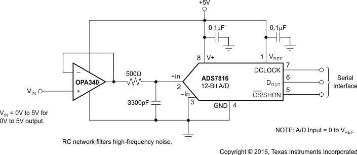
The OPA340 series rail-to-rail CMOS operational amplifiers are optimized for low-voltage, single-supply operation. Rail-to-rail input and output and high-speed operation make them ideal for driving sampling analog-to-digital (A/D) converters. They are also well-suited for general purpose and audio applications as well as providing I/V conversion at the output of digital-to-analog (D/A) converters. Single, dual, and quad versions have identical specifications for design flexibility.
The OPA340 series operate on a single supply as low as 2.5 V with an input common-mode voltage range that extends 500 mV below ground and 500 mV above the positive supply. Output voltage swing is to within 1 mV of the supply rails with a 100-kΩ load. These devices offer excellent dynamic response
(BW = 5.5 MHz, SR = 6 V/µs), yet quiescent current is only 750 A. Dual and quad designs feature completely independent circuitry for lowest crosstalk and freedom from interaction.
The single (OPA340) packages are the tiny 5-pin SOT-23 surface mount, 8-pin SOIC surface mount, and 8-pin DIP. The dual (OPA2340) comes in the miniature 8-pin VSSOP surface mount, 8-pin SOIC surface mount, and 8-pin PDIP packages. The quad (OPA4340) packages are the space-saving 16-pin SSOP surface mount and 14-pin SOIC surface mount. All are specified from –40°C to 85°C and operate from –55°C to 125°C. A SPICE macromodel is available for design analysis.
PART NUMBER | PACKAGE | BODY SIZE (NOM) |
---|---|---|
OPA340 | SOT-23 (5) | 3.00 mm × 3.00 mm |
OPA340, OPA2340 | PDIP (8) | 9.81 mm × 6.35 mm |
SOIC (8) | 4.90 mm × 3.91 mm | |
OPA2340 | VSSOP (8) | 3.00 mm × 3.00 mm |
OPA4340 | SOIC (14) | 8.65 mm × 3.91 mm |
SSOP (16) | 4.90 mm × 3.90 mm |
Changes from B Revision (November 2007) to C Revision
PIN | I/O | DESCRIPTION | ||
---|---|---|---|---|
NAME | SOT-23 | SOIC, PDIP | ||
–IN | 4 | 2 | I | Negative (inverting) input |
+IN | 3 | 3 | I | Positive (noninverting) input |
NC | — | 1, 5, 8 | — | No internal connection (can be left floating) |
OUT | 1 | 6 | O | Output |
V– | 2 | 4 | — | Negative (lowest) power supply |
V+ | 5 | 7 | — | Positive (highest) power supply |
PIN | I/O | DESCRIPTION | |
---|---|---|---|
NAME | VSSOP, SOIC, PDIP | ||
–IN A | 2 | I | Negative (inverting) input channel A |
+IN A | 3 | I | Positive (noninverting) input channel A |
–IN B | 6 | I | Negative (inverting) input channel B |
+IN B | 5 | I | Positive (noninverting) input channel B |
OUT A | 1 | O | Output channel A |
OUT B | 7 | O | Output channel B |
V– | 4 | — | Negative (lowest) power supply |
V+ | 8 | — | Positive (highest) power supply |
PIN | I/O | DESCRIPTION | ||
---|---|---|---|---|
NAME | SOIC | SSOP | ||
–IN A | 2 | 2 | I | Negative (inverting) input channel A |
–IN B | 6 | 6 | I | Negative (inverting) input channel B |
–IN C | 9 | 11 | I | Negative (inverting) input channel C |
–IN D | 13 | 15 | I | Negative (inverting) input channel D |
+IN A | 3 | 3 | I | Positive (noninverting) input channel A |
+IN B | 5 | 5 | I | Positive (noninverting) input channel B |
+IN C | 10 | 12 | I | Positive (noninverting) input channel C |
+IN D | 12 | 14 | I | Positive (noninverting) input channel D |
NC | — | 8, 9 | — | No internal connection (can be left floating) |
OUT A | 1 | 1 | O | Output, channel A |
OUT B | 7 | 7 | O | Output, channel B |
OUT C | 8 | 10 | O | Output, channel C |
OUT D | 14 | 16 | O | Output, channel D |
V– | 11 | 13 | — | Negative (lowest) power supply |
V+ | 4 | 4 | — | Positive (highest) power supply |
MIN | MAX | UNIT | |||
---|---|---|---|---|---|
Voltage | Supply voltage | 5.5 | V | ||
Signal input terminals(2) | –0.5 | 0.5 | |||
Current | Signal input terminals(2) | 10 | mA | ||
Output short circuit(3) | Continuous | ||||
Temperature | Operating, TA | –55 | 125 | °C | |
Junction, TJ | 150 | ||||
Storage, Tstg | –55 | 125 |
VALUE | UNIT | |||
---|---|---|---|---|
V(ESD) | Electrostatic discharge | Human-body model (HBM), per ANSI/ESDA/JEDEC JS-001(1) | ±600 | V |
Charged-device model (CDM), per JEDEC specification JESD22-C101(2) | ±250 |
MIN | MAX | UNIT | ||
---|---|---|---|---|
Supply voltage | 2.7 | 5.5 | V | |
Specified temperature | –40 | 125 | °C |
THERMAL METRIC(1) | OPA340 | UNIT | ||||
---|---|---|---|---|---|---|
DBV (SOT-23) |
P (PDIP) |
D (SOIC) |
D (SOIC) |
|||
5 PINS | 8 PINS | 8 PINS | 14 PINS | |||
RθJA | Junction-to-ambient thermal resistance | 207.9 | 53.1 | 142 | 83.8 | °C/W |
RθJC(top) | Junction-to-case (top) thermal resistance | 71.2 | 42.5 | 90.2 | 70.7 | °C/W |
RθJB | Junction-to-board thermal resistance | 36.0 | 30.3 | 82.5 | 59.5 | °C/W |
ψJT | Junction-to-top characterization parameter | 2.0 | 19.7 | 39.4 | 11.6 | °C/W |
ψJB | Junction-to-board characterization parameter | 35.2 | 30.2 | 82 | 37.7 | °C/W |
RθJC(bot) | Junction-to-case (bottom) thermal resistance | — | — | — | — | °C/W |
THERMAL METRIC(1) | OPA2340 | UNIT | ||
---|---|---|---|---|
D (SOIC) |
DGK (VSSOP) |
|||
8 PINS | 8 PINS | |||
RθJA | Junction-to-ambient thermal resistance | 138.4 | 169.2 | °C/W |
RθJC(top) | Junction-to-case (top) thermal resistance | 89.5 | 62.8 | °C/W |
RθJB | Junction-to-board thermal resistance | 78.6 | 89.8 | °C/W |
ψJT | Junction-to-top characterization parameter | 29.9 | 7.5 | °C/W |
ψJB | Junction-to-board characterization parameter | 78.1 | 88.2 | °C/W |
RθJC(bot) | Junction-to-case (bottom) thermal resistance | — | — | °C/W |
THERMAL METRIC(1) | OPA4340 | UNIT | |
---|---|---|---|
DBQ (SSOP) |
|||
16 PINS | |||
RθJA | Junction-to-ambient thermal resistance | 115.8 | °C/W |
RθJC(top) | Junction-to-case (top) thermal resistance | 67 | °C/W |
RθJB | Junction-to-board thermal resistance | 58.3 | °C/W |
ψJT | Junction-to-top characterization parameter | 19.9 | °C/W |
ψJB | Junction-to-board characterization parameter | 57.9 | °C/W |
RθJC(bot) | Junction-to-case (bottom) thermal resistance | — | °C/W |
PARAMETER | TEST CONDITIONS | MIN | TYP(1) | MAX | UNIT | ||
---|---|---|---|---|---|---|---|
OFFSET VOLTAGE | |||||||
VOS | Input offset voltage | VS = 5 V | ±150 | ±500 | µV | ||
dVOS/dt | Input offset voltage vs temperature | TA = –40°C to 85°C, VS = 5 V | ±2.5 | µV/°C | |||
PSRR | Input offset voltage vs power supply | VS = 2.7 V to 5.5 V, VCM = 0 V | 30 | 120 | µV/V | ||
Over temperature | VS = 2.7 V to 5.5 V, VCM = 0 V, TA = –40°C to 85°C, VS = 5 V |
120 | µV/°C | ||||
Channel separation, DC | 0.2 | µV/V | |||||
INPUT BIAS CURRENT | |||||||
IS | Input bias current | ±0.2 | ±10 | pA | |||
Over temperature | TA = –40°C to 85°C, VS = 5 V | ±60 | |||||
IOS | Input offset current | ±0.2 | ±10 | pA | |||
NOISE | |||||||
Input voltage noise | f = 0.1 kHz to 50 kHz | 8 | µVRMS | ||||
en | Input voltage noise density | f = 1 kHz | 25 | nV/√Hz | |||
in | Current noise density | f = 1 kHz | 3 | fA/√Hz | |||
INPUT VOLTAGE RANGE | |||||||
VCM | Common-mode voltage range | –0.3 | (V+) + 0.3 | V | |||
CMRR | Common-mode rejection ratio | –0.3 V < VCM < (V+) – 1.8 V | 80 | 92 | dB | ||
VS = 5 V, –0.3 V < VCM < 5.3 V | 70 | 84 | |||||
VS = 2.7 V, –0.3 V < VCM < 3 V | 66 | 80 | |||||
INPUT IMPEDANCE | |||||||
Differential | 1013 || 3 | Ω || pF | |||||
Common-mode | 1013 || 6 | Ω || pF | |||||
OPEN-LOOP GAIN | |||||||
AOL | Open-loop voltage gain | RL = 100 kΩ, 5 mV < VO < (V+) – 5 mV |
106 | 124 | dB | ||
RL = 10 kΩ, 5 mV < VO < (V+) – 50 mV |
100 | 120 | |||||
RL = 2 kΩ, 200 mV < VO < (V+) – 200 mV |
94 | 114 | |||||
Over temperature | RL = 100 kΩ, 5 mV < VO < (V+) – 5 mV, TA = –40°C to 85°C, VS = 5 V |
106 | |||||
RL = 10 kΩ, 5 mV < VO < (V+) – 50 mV, TA = –40°C to 85°C, VS = 5 V |
100 | ||||||
RL = 2 kΩ, 200 mV < VO < (V+) – 200 mV, TA = –40°C to 85°C, VS = 5 V |
94 | ||||||
FREQUENCY RESPONSE | |||||||
GBW | Gain-bandwidth product | G = 1 | 5.5 | MHz | |||
SR | Slew rate | VS = 5 V, G = 1, CL = 100 pF | 6 | V/µs | |||
Settling time, 0.1% | VS = 5 V, 2-V step, CL = 100 pF | 1 | µs | ||||
Settling time, 0.01% | VS = 5 V, 2-V step, CL = 100 pF | 1.6 | µs | ||||
Overload recovery time | VIN × G = VS | 0.2 | µs | ||||
THD+N | Total harmonic distortion + noise | VS = 5 V, VO = 3VPP(2), G = 1, f = 1 kHz |
0.0007% | ||||
OUTPUT | |||||||
Voltage output swing from rail(2) | RL = 100 kΩ, AOL ≥ 106 dB | 1 | 5 | mV | |||
RL = 10 kΩ, AOL ≥ 106 dB | 10 | ||||||
RL = 2 kΩ, AOL ≥ 106 dB | 40 | ||||||
Over temperature | RL = 100 kΩ, AOL ≥ 106 dB, TA = –40°C to 85°C, VS = 5 V |
5 | |||||
RL = 10 kΩ, AOL ≥ 106 dB, TA = –40°C to 85°C, VS = 5 V |
50 | ||||||
RL = 2 kΩ, AOL ≥ 106 dB, TA = –40°C to 85°C, VS = 5 V |
200 | ||||||
ISC | Short-circuit current | ±50 | mA | ||||
CLOAD | Capacitive load drive | See Typical Characteristics | |||||
POWER SUPPLY | |||||||
VS | Specified voltage range | 2.7 | 5 | V | |||
Operating voltage range | Lower end | 2.5 | V | ||||
Higher end | 5.5 | ||||||
IQ | Quiescent current (per amplifier) |
IO = 0, VS = 5 V | 750 | 950 | µA | ||
Over temperature | IO = 0, VS = 5 V, TA = –40°C to 85°C | 100 | |||||
TEMPERATURE RANGE | |||||||
Specified range | –40 | 85 | °C | ||||
Operating range | –55 | 125 | °C | ||||
Storage range | –55 | 125 | °C |
CL = 100 pF |
CL = 100 pF |