-
OPAx377-Q1 Low-Noise, Low Quiescent Current, Precision Automotive Grade Operational Amplifier SBOS797A May 2016 – May 2016 OPA2377-Q1 , OPA377-Q1 , OPA4377-Q1
PRODUCTION DATA.
-
OPAx377-Q1 Low-Noise, Low Quiescent Current, Precision Automotive Grade Operational Amplifier
- 1 Features
- 2 Applications
- 3 Description
- 4 Revision History
- 5 Pin Configuration and Functions
- 6 Specifications
- 7 Detailed Description
- 8 Application and Implementation
- 9 Power Supply Recommendations
- 10Layout
- 11Device and Documentation Support
- 12Mechanical, Packaging, and Orderable Information
- IMPORTANT NOTICE
Package Options
Mechanical Data (Package|Pins)
- DBV|5
Thermal pad, mechanical data (Package|Pins)
Orderable Information
OPAx377-Q1 Low-Noise, Low Quiescent Current, Precision Automotive Grade Operational Amplifier
1 Features
- Qualified for Automotive Applications
- AEC-Q100 Qualified with the Following Results:
- Device Temperature Grade 1: –40°C to +125°C Ambient Operating Temperature Range
- Device HBM ESD Classification Level 3A
- Device CDM ESD Classification Level C6
- Low Noise: 7.5 nV/√Hz at 1 kHz
- 0.1-Hz to 10-Hz Noise: 0.8 μVPP
- Quiescent Current: 760 μA (typical)
- Low Offset Voltage: 250 μV (typical)
- Gain Bandwidth Product: 5.5 MHz
- Rail-to-Rail Input and Output
- Single-Supply Operation
- Supply Voltage: 2.2 V to 5.5 V
- Space-Saving Packages:
- SOT-23, VSSOP, TSSOP
2 Applications
- Active Cruise Control
- Park Assist
- Tire Pressure Monitoring
- Infotainment
- Active Filtering
- Sensor Signal Conditioning
3 Description
The OPAx377-Q1 family of operational amplifiers are wide-bandwidth CMOS amplifiers that provide very low noise, low input bias current, and low offset voltage while operating on a low quiescent current of 0.76 mA (typical).
The OPAx377-Q1 op amps are optimized for low-voltage, single-supply applications. The exceptional combination of ac and dc performance make them ideal for a wide range of applications, including small signal conditioning, audio, and active filters. In addition, these parts have a wide supply range with excellent PSRR, making them attractive for applications that run directly from batteries without regulation.
The OPA377-Q1 is available in the SOT23-5 package. The dual, OPA2377-Q1, is offered in the MSOP-8 package and the quad OPA4377-Q1 is offered in the TSSOP-14 package. All versions are specified for operation from –40°C to +125°C.
Device Information(1)
| PART NUMBER | PACKAGE | BODY SIZE (NOM) |
|---|---|---|
| OPA377-Q1 | SOT-23 (5) | 2.90 mm × 1.60 mm |
| OPA2377-Q1 | VSSOP (8) | 3.00 mm × 3.00 mm |
| OPA4377-Q1 | TSSOP (14) | 5.00 mm × 4.40 mm |
- For all available packages, see the orderable addendum at the end of the data sheet.
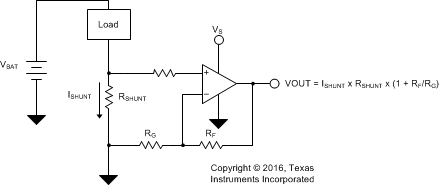
Low-Side Current Sense Amplifier

4 Revision History
Changes from * Revision (May 2016) to A Revision
- Changed device status from Product Preview to Production Data Go
5 Pin Configuration and Functions

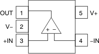
Pin Functions: OPA377-Q1
| PIN | I/O | DESCRIPTION | |
|---|---|---|---|
| NAME | NO. | ||
| DBV | |||
| +IN | 3 | I | Noninverting input |
| –IN | 4 | I | Inverting input |
| NC | — | — | No internal connection (can be left floating) |
| OUT | 1 | O | Output |
| V– | 2 | — | Negative (lowest) power supply |
| V+ | 5 | — | Positive (highest) power supply |

Pin Functions: OPA2377-Q1
| PIN | I/O | DESCRIPTION | |
|---|---|---|---|
| NAME | NO. | ||
| DGK | |||
| –IN A | 2 | I | Inverting input, channel A |
| –IN B | 6 | I | Inverting input, channel B |
| +IN A | 3 | I | Noninverting input, channel A |
| +IN B | 5 | I | Noninverting input, channel B |
| OUT A | 1 | O | Output, channel A |
| OUT B | 7 | O | Output, channel B |
| V– | 4 | — | Negative (lowest) power supply |
| V+ | 8 | — | Positive (highest) power supply |

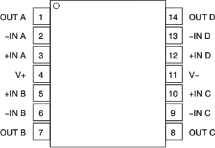
Pin Functions: OPA4377-Q1
| PIN | I/O | DESCRIPTION | |
|---|---|---|---|
| NAME | NO. | ||
| PW | |||
| –IN A | 2 | I | Inverting input, channel A |
| –IN B | 6 | I | Inverting input, channel B |
| –IN C | 9 | I | Inverting input, channel C |
| –IN D | 13 | I | Inverting input, channel D |
| +IN A | 3 | I | Noninverting input, channel A |
| +IN B | 5 | I | Noninverting input, channel B |
| +IN C | 10 | I | Noninverting input, channel C |
| +IN D | 12 | I | Noninverting input, channel D |
| OUT A | 1 | O | Output, channel A |
| OUT B | 7 | O | Output, channel B |
| OUT C | 8 | O | Output, channel C |
| OUT D | 14 | O | Output, channel D |
| V– | 11 | — | Negative (lowest) power supply |
| V+ | 4 | — | Positive (highest) power supply |