-
OPAx316-Q1 10-MHz, Rail-to-Rail Input/Output, Low-Voltage, 1.8-V CMOS Operational Amplifier SBOS841A November 2016 – January 2017 OPA2316-Q1 , OPA316-Q1 , OPA4316-Q1
PRODUCTION DATA.
-
OPAx316-Q1 10-MHz, Rail-to-Rail Input/Output, Low-Voltage, 1.8-V CMOS Operational Amplifier
- 1 Features
- 2 Applications
- 3 Description
- 4 Revision History
- 5 Pin Configuration and Functions
- 6 Specifications
- 7 Detailed Description
- 8 Application and Implementation
- 9 Power Supply Recommendations
- 10Layout
- 11Device and Documentation Support
- 12Mechanical, Packaging, and Orderable Information
- IMPORTANT NOTICE
Package Options
Mechanical Data (Package|Pins)
- PW|14
Thermal pad, mechanical data (Package|Pins)
Orderable Information
OPAx316-Q1 10-MHz, Rail-to-Rail Input/Output, Low-Voltage, 1.8-V CMOS Operational Amplifier
1 Features
- Qualified for Automotive Applications
- AEC-Q100 Qualified With the Following Results:
- Unity-Gain Bandwidth: 10 MHz
- Low IQ: 400 µA/ch
- Wide Supply Range: 1.8 V to 5.5 V
- Low Noise: 11 nV/√Hz at 1 kHz
- Low Input Bias Current: ±5 pA
- Offset Voltage: ±0.5 mV
- Unity-Gain Stable
- Internal RFI-EMI Filter
- Extended Temperature Range: –40°C to +125°C
2 Applications
- Automotive Applications:
- ADAS
- Body Electronics and Lighting
- Current Sensing
- Battery Management Systems
3 Description
The OPAx316-Q1 family of single and dual operational amplifiers represents a new generation of general-purpose, low-power operational amplifiers. Featuring rail-to-rail input and output swings, low quiescent current (400 μA/ch typical) combined with a wide bandwidth of 10 MHz and very-low noise
(11 nV/√Hz at 1 kHz) makes this family suitable for circuits requiring a good speed and power ratio. The low input bias current supports those operational amplifiers for applications with megaohm source impedances. The low input bias current of the OPAx316-Q1 yields a very-low current noise to make the device attractive for high impedance sensor interfaces.
The robust design of the OPAx316-Q1 provides ease-of-use to the circuit designer: a unity-gain stable, integrated RFI and EMI rejection filter, no phase reversal in overdrive condition, and high electrostatic discharge (ESD) protection (4-kV HBM).
These devices are optimized for low-voltage operation as low as 1.8 V (±0.9 V) and up to 5.5 V (±2.75 V). This latest addition of low-voltage CMOS automotive grade operational amplifiers provide a family of wide bandwidth, low noise, and low power that meet the needs of a wide variety of applications.
Device Information(1)
| PART NUMBER | PACKAGE | BODY SIZE (NOM) |
|---|---|---|
| OPA316-Q1 | SOT-23 (5) | 1.60 mm × 2.90 mm |
| OPA2316-Q1 | VSSOP (8) | 3.00 mm × 3.00 mm |
| OPA4316-Q1 | TSSOP (14) | 4.40 mm × 5.00 mm |
- For all available packages, see the orderable addendum at the end of the data sheet.
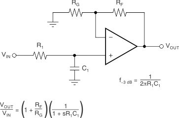
Single-Pole, Low-Pass Filter
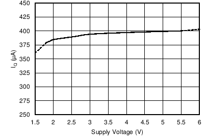
Low-Supply Current (400 µA/ch) for 10-MHz Bandwidth
4 Revision History
Changes from * Revision (November 2016) to A Revision
- Changed CDM classification reduced from C6 Go
- Deleted OPA2316S-Q1 package and body size information from Device Information table Go
- Deleted SC70 (5) (OPA316-Q1), DFN (8), MSOP (8), SOIC (8) (OPA2316-Q1), and SOIC (14) packages (OPA4316-Q1) from the Device Information table, Thermal Information tables, and pinout diagramsGo
- Deleted OPA2316S-Q1 pin diagram and Pin Functions table in Pin Configurations and Functions section Go
- Deleted D (SOIC) package from OPA4316-Q1 pin diagram in Pin Configurations and Functions section Go
- Changed CDM rating from ±1500 V to ±750 VGo
- Deleted OPA2316S-Q1 device thermal information in the Thermal Information table Go
- Added thermal information for OPA4316-Q1 deviceGo
- Deleted the literature numbers in parentheses from the format of TI document references in the Documentation Support section Go
5 Pin Configuration and Functions
Pin Functions: OPA316-Q1
| PIN | I/O | DESCRIPTION | |
|---|---|---|---|
| NAME | NO. | ||
| –IN | 4 | I | Inverting input |
| +IN | 3 | I | Noninverting input |
| V– | 2 | — | Negative supply or ground (for single-supply operation). |
| V+ | 5 | — | Positive supply |
| OUT | 1 | O | Output |
Pin Functions: OPA2316-Q1
| PIN | I/O | DESCRIPTION | |
|---|---|---|---|
| NAME | NO. | ||
| –IN A | 2 | I | Inverting input, channel A |
| +IN A | 3 | I | Noninverting input, channel A |
| –IN B | 6 | I | Inverting input, channel B |
| +IN B | 5 | I | Noninverting input, channel B |
| OUT A | 1 | O | Output, channel A |
| OUT B | 7 | O | Output, channel B |
| V– | 4 | — | Negative supply or ground (for single-supply operation). |
| V+ | 8 | — | Positive supply |
Pin Functions: OPA4316-Q1
| PIN | I/O | DESCRIPTION | |
|---|---|---|---|
| NAME | NO. | ||
| –IN A | 2 | I | Inverting input, channel A |
| +IN A | 3 | I | Noninverting input, channel A |
| –IN B | 6 | I | Inverting input, channel B |
| +IN B | 5 | I | Noninverting input, channel B |
| –IN C | 9 | I | Inverting input, channel C |
| +IN C | 10 | I | Noninverting input, channel C |
| –IN D | 13 | I | Inverting input, channel D |
| +IN D | 12 | I | Noninverting input, channel D |
| OUT A | 1 | O | Output, channel A |
| OUT B | 7 | O | Output, channel B |
| OUT C | 8 | O | Output, channel C |
| OUT D | 14 | O | Output, channel D |
| V– | 11 | — | Negative supply or ground (for single-supply operation) |
| V+ | 4 | — | Positive supply |
6 Specifications
6.1 Absolute Maximum Ratings
over operating free-air temperature (unless otherwise noted)(1)| MIN | MAX | UNIT | |||
|---|---|---|---|---|---|
| Supply voltage | 7 | V | |||
| Signal input pins | Voltage(2) | Common-mode | (V–) – 0.5 | (V+) + 0.5 | V |
| Differential | (V+) – (V–) + 0.2 | V | |||
| Current(2) | –10 | 10 | mA | ||
| Output short-circuit(3) | Continuous | ||||
| TA | Operating temperature | –55 | 150 | °C | |
| TJ | Junction temperature | 150 | °C | ||
| Tstg | Storage temperature | –65 | 150 | °C | |
6.2 ESD Ratings
| VALUE | UNIT | |||
|---|---|---|---|---|
| V(ESD) | Electrostatic discharge | Human-body model (HBM), per AEC Q100-002(1) | ±4000 | V |
| Charged-device model (CDM), per AEC Q100-011 | ±750 | |||
6.3 Recommended Operating Conditions
over operating free-air temperature range (unless otherwise noted)| MIN | MAX | UNIT | |||
|---|---|---|---|---|---|
| VS | Supply voltage | 1.8 | 5.5 | V | |
| Specified temperature | –40 | 125 | °C | ||
6.4 Thermal Information: OPA316-Q1
| THERMAL METRIC(1) | OPA316-Q1 | UNIT | |
|---|---|---|---|
| DBV (SOT-23) | |||
| 5 PINS | |||
| RθJA | Junction-to-ambient thermal resistance(2) | 221.7 | °C/W |
| RθJC(top) | Junction-to-case(top) thermal resistance(3) | 144.7 | °C/W |
| RθJB | Junction-to-board thermal resistance(4) | 49.7 | °C/W |
| ψJT | Junction-to-top characterization parameter(5) | 26.1 | °C/W |
| ψJB | Junction-to-board characterization parameter(6) | 49 | °C/W |
| RθJC(bot) | Junction-to-case(bottom) thermal resistance(7) | N/A | °C/W |
6.5 Thermal Information: OPA2316-Q1
| THERMAL METRIC(1) | OPA2316-Q1 | UNIT | |
|---|---|---|---|
| DGK (VSSOP) | |||
| 8 PINS | |||
| RθJA | Junction-to-ambient thermal resistance(2) | 186.6 | °C/W |
| RθJC(top) | Junction-to-case(top) thermal resistance(3) | 78.8 | °C/W |
| RθJB | Junction-to-board thermal resistance(4) | 107.9 | °C/W |
| ψJT | Junction-to-top characterization parameter(5) | 15.5 | °C/W |
| ψJB | Junction-to-board characterization parameter(6) | 106.3 | °C/W |
| RθJC(bot) | Junction-to-case(bottom) thermal resistance(7) | N/A | °C/W |
6.6 Thermal Information: OPA4316-Q1
| THERMAL METRIC(1) | OPA4316-Q1 | UNIT | |
|---|---|---|---|
| PW (TSSOP) | |||
| 14 PINS | |||
| RθJA | Junction-to-ambient thermal resistance(2) | 117.2 | °C/W |
| RθJC(top) | Junction-to-case(top) thermal resistance(3) | 46.2 | °C/W |
| RθJB | Junction-to-board thermal resistance(4) | 58.9 | °C/W |
| ψJT | Junction-to-top characterization parameter(5) | 4.9 | °C/W |
| ψJB | Junction-to-board characterization parameter(6) | 58.3 | °C/W |
| RθJC(bot) | Junction-to-case(bottom) thermal resistance(2) | N/A | °C/W |
6.7 Electrical Characteristics
VS (total supply voltage) = (V+) – (V–) = 1.8 V to 5.5 V.at TA = 25°C, RL = 10 kΩ connected to VS / 2, VCM = VS / 2, and VOUT = VS / 2, unless otherwise noted
| PARAMETER | TEST CONDITIONS | MIN | TYP | MAX | UNIT | ||
|---|---|---|---|---|---|---|---|
| OFFSET VOLTAGE | |||||||
| VOS | Input offset voltage | VS = 5 V | ±0.5 | ±2.5 | mV | ||
| VS = 5 V, TA = –40°C to 125°C | ±3.5 | mV | |||||
| dVOS/dT | Drift | VS = 5 V, TA = –40°C to 125°C | ±2 | ±10 | μV/°C | ||
| PSRR | vs power supply | VS = 1.8 V – 5.5 V, VCM = (V–) | ±30 | ±150 | µV/V | ||
| VS = 1.8 V – 5.5 V, VCM = (V–), TA = –40°C to 125°C | ±250 | µV/V | |||||
| Channel separation, dc | At dc | 10 | µV/V | ||||
| INPUT VOLTAGE RANGE | |||||||
| VCM | Common-mode voltage | VS = 1.8 V to 2.5 V | (V–) – 0.2 | (V+) | V | ||
| VS = 2.5 V to 5.5 V | (V–) – 0.2 | (V+) + 0.2 | V | ||||
| CMRR | Common-mode rejection ratio | VS = 1.8 V, (V–) – 0.2 V < VCM < (V+) – 1.4 V, TA= –40°C to 125°C |
70 | 86 | dB | ||
| VS = 5.5 V, (V–) – 0.2 V < VCM < (V+) – 1.4 V, TA= –40°C to 125°C |
76 | 90 | dB | ||||
| VS = 1.8 V, VCM = –0.2 V to 1.8 V, TA= –40°C to 125°C |
57 | 72 | dB | ||||
| VS = 5.5 V, VCM = –0.2 V to 5.7 V, TA= –40°C to 125°C |
65 | 80 | dB | ||||
| INPUT BIAS CURRENT | |||||||
| IB | Input bias current | ±5 | ±15 | pA | |||
| TA= –40°C to 125°C | ±15 | nA | |||||
| IOS | Input offset current | ±2 | ±15 | pA | |||
| TA= –40°C to 125°C | ±8 | nA | |||||
| NOISE | |||||||
| En | Input voltage noise (peak-to-peak) | VS = 5 V, f = 0.1 Hz to 10 Hz | 3 | μVPP | |||
| en | Input voltage noise density | VS = 5 V, f = 1 kHz | 11 | nV/√Hz | |||
| in | Input current noise density | f = 1 kHz | 1.3 | fA/√Hz | |||
| INPUT IMPEDANCE | |||||||
| ZID | Differential | 2 || 2 | 1016Ω || pF | ||||
| ZIC | Common-mode | 2 || 4 | 1011Ω || pF | ||||
| OPEN-LOOP GAIN | |||||||
| AOL | Open-loop voltage gain | VS = 1.8 V, (V–) + 0.04 V < VO < (V+) – 0.04 V, RL = 10 kΩ |
94 | 100 | dB | ||
| VS = 5.5 V, (V–) + 0.05 V < VO < (V+) – 0.05 V, RL = 10 kΩ |
104 | 110 | dB | ||||
| VS = 1.8 V, (V–) + 0.1 V < VO < (V+) – 0.1 V, RL = 2 kΩ |
90 | 96 | dB | ||||
| VS = 5.5 V, (V–) + 0.15 V < VO < (V+) – 0.15 V, RL = 2 kΩ |
100 | 106 | dB | ||||
| VS = 5.5 V, (V–) + 0.05 V < VO < (V+) – 0.05 V, RL = 10 kΩ, TA= –40°C to 125°C |
86 | dB | |||||
| VS = 5.5 V, (V–) + 0.15 V < VO < (V+) – 0.15 V, RL = 2 kΩ, TA= –40°C to 125°C |
84 | dB | |||||
| FREQUENCY RESPONSE | |||||||
| GBP | Gain bandwidth product | VS = 5 V, G = 1 | 10 | MHz | |||
| φm | Phase margin | VS = 5 V, G = 1 | 60 | Degrees | |||
| SR | Slew rate | VS = 5 V, G = 1 | 6 | V/μs | |||
| tS | Settling time | To 0.1%, VS = 5 V, 2-V step , G = 1, CL = 100 pF | 1 | μs | |||
| To 0.01%, VS = 5 V, 2-V step , G = 1, CL = 100 pF | 1.66 | μs | |||||
| tOR | Overload recovery time | VS = 5 V, VIN × gain = VS | 0.3 | μs | |||
| THD + N | Total harmonic distortion + noise(1) | VS = 5 V, VO = 0.5 VRMS, G = 1 f = 1 kHz |
0.0008% | ||||
| OUTPUT | |||||||
| VO | Voltage output swing from supply rails | VS = 1.8 V, RL = 10 kΩ, TA= –40°C to 125°C | 15 | mV | |||
| VS = 5.5 V, RL = 10 kΩ, TA= –40°C to 125°C | 30 | mV | |||||
| VS = 1.8 V, RL = 2 kΩ, TA= –40°C to 125°C | 60 | mV | |||||
| VS = 5.5 V, RL = 2 kΩ, TA= –40°C to 125°C | 120 | mV | |||||
| ISC | Short-circuit current | VS = 5 V | ±50 | mA | |||
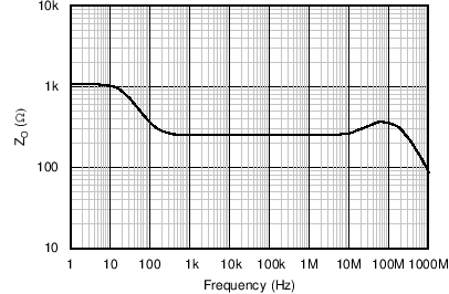
| ZO | Open-loop output impedance | VS = 5 V, f = 10 MHz | 250 | Ω | |||
| POWER SUPPLY | |||||||
| VS | Specified voltage | 1.8 | 5.5 | V | |||
| IQ | Quiescent current per amplifier | VS = 5 V, IO = 0 mA, TA= –40°C to 125°C | 400 | 500 | µA | ||
| Power-on time | VS = 0 V to 5.5 V | 200 | µs | ||||
6.8 Typical Characteristics
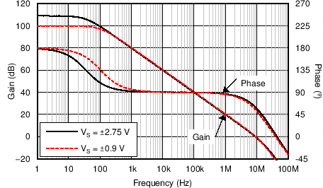
at TA = 25°C, VS = 5.5 V, RL = 10 kΩ connected to VS / 2, VCM = VS / 2, and VOUT = VS / 2, unless otherwise noted.
| Distribution taken from 12551 amplifiers | ||

| 9 typical units shown | ||

| V+ = 0.9 V to 2.75 V, V– = –0.9 V to –2.75 V, 9 typical units shown |

| RL = 10 kΩ | ||


| V+ = 2.75 V, V– = –2.75 V | ||


| Bandwidth = 80 kHz, VOUT = 0.5 VRMS | ||

| V+ = 2.75 V | G = +1 V/V | RL = 1 kΩ |
| V– = –2.75 V |

| V+ = 2.75 V | V– = –2.75 V | G = –10 V/V |

| V+ = 2.75 V | V– = –2.75 V | G = +1 V/V |

| CL = 100 pF | G = +1 V/V |


| PRF = –10 dBm | ||
Referred to Noninverting Input (EMIRR IN+) vs Frequency

| TA = –40°C to +125°C, Distribution taken from 70 amplifiers | ||

| V+ = 2.75 V, V– = –2.75 V, 9 typical units shown | ||

| VCM < (V+) – 1.4 V | ||

| RL = 2 kΩ | ||


(Referred to Input)


| ƒ = 1 kHz | ||

| ƒ = 1 kHz, Bandwidth = 80 kHz | ||


| V+ = 2.75 V | V– = –2.75 V | G = –1 V/V |

| V+ = 2.75 V | V– = –2.75 V | |

| V+ = 2.75 V | V– = –2.75 V | G = –10 V/V |

| V+ = 2.75 V | CL = 100 pF | G = +1 V/V |
| V– = –2.75 V |

| CL = 100 pF | G = +1 V/V |

Frequency and Supply Voltage

| V+ = 2.75 V, V– = –2.75 V | ||
7 Detailed Description
7.1 Overview
The OPAx316-Q1 is a family of low-power, rail-to-rail input and output operational amplifiers. These devices operate from 1.8 V to 5.5 V, are unity-gain stable, and are suitable for a wide range of general-purpose applications. The class AB output stage is capable of driving less than or equal to 10-kΩ loads connected to any point between V+ and ground. The input common-mode voltage range includes both rails and allows the OPAx316-Q1 series to be used in virtually any single-supply application. Rail-to-rail input and output swing significantly increases dynamic range, especially in low-supply applications, and makes them suitable for driving sampling analog-to-digital converters (ADCs).
The OPAx316-Q1 family features 10-MHz bandwidth and 6-V/μs slew rate with only 400-μA supply current per channel, providing good ac performance at very-low-power consumption. DC applications are well served with a very-low input noise voltage of 11 nV/√Hz at 1 kHz, low input bias current (5 pA), and a typical input offset voltage of 0.5-mV.
7.2 Functional Block Diagram

7.3 Feature Description
7.3.1 Operating Voltage
The OPAx316-Q1 operational amplifiers are fully specified and ensured for operation from 1.8 V to 5.5 V. In addition, many specifications apply from –40°C to +125°C. Parameters that vary significantly with operating voltages or temperature are illustrated in the Typical Characteristics graphs.
7.3.2 Rail-to-Rail Input
The input common-mode voltage range of the OPAx316-Q1 series extends 200 mV beyond the supply rails for supply voltages greater than 2.5 V. This performance is achieved with a complementary input stage: an N-channel input differential pair in parallel with a P-channel differential pair, as shown in the Functional Block Diagram. The N-channel pair is active for input voltages close to the positive rail, typically (V+) – 1.4 V to 200 mV above the positive supply, whereas the P-channel pair is active for inputs from 200 mV below the negative supply to approximately (V+) – 1.4 V. There is a small transition region, typically (V+) – 1.2 V to (V+) – 1 V, in which both pairs are on. This 200-mV transition region can vary up to 200 mV with process variation. Thus, the transition region (both stages on) can range from (V+) – 1.4 V to (V+) – 1.2 V on the low end, up to (V+) – 1 V to (V+) – 0.8 V on the high end. Within this transition region, PSRR, CMRR, offset voltage, offset drift, and THD can degrade compared to device operation outside this region.
7.3.3 Input and ESD Protection
The OPAx316-Q1 incorporates internal ESD protection circuits on all pins. In the case of input and output pins, this protection primarily consists of current-steering diodes connected between the input and power-supply pins. These ESD protection diodes provide in-circuit, input overdrive protection, as long as the current is limited to 10 mA, as stated in Absolute Maximum Ratings table. Figure 37 shows how a series input resistor can be added to the driven input to limit the input current. The added resistor contributes thermal noise at the amplifier input and the value must be kept to a minimum in noise-sensitive applications.
 Figure 37. Input Current Protection
7.3.4 Common-Mode Rejection Ratio (CMRR)
CMRR for the OPAx316-Q1 is specified in several ways so the user can select the best match for a given application, as shown in the Electrical Characteristics table. First, the data sheet gives the CMRR of the device in the common-mode range below the transition region [VCM < (V+) – 1.4 V]. This specification is the best indicator of device capability when the application requires use of one of the differential input pairs. Second, the CMRR over the entire common-mode range is specified at VCM = –0.2 V to 5.7 V for VS = 5.5 V. This last value includes the variations shown in Figure 4 through the transition region.
7.3.5 EMI Susceptibility and Input Filtering
Operational amplifiers vary with regard to the susceptibility of the device to electromagnetic interference (EMI). If conducted EMI enters the operational amplifier, the dc offset observed at the amplifier output can shift from the nominal value when EMI is present. This shift is a result of signal rectification associated with the internal semiconductor junctions. Although EMI can affect all operational amplifier pin functions, the signal input pins are likely to be the most susceptible. The OPA316-Q1 operational amplifier family incorporates an internal input low-pass filter that reduces the amplifier response to EMI. This filter provides both common-mode and differential-mode filtering. The filter is designed for a cutoff frequency of approximately 80 MHz (–3 dB), with a roll-off of 20 dB per decade.
TI developed the ability to accurately measure and quantify the immunity of an operational amplifier over a broad frequency spectrum extending from 10 MHz to 6 GHz. The EMI rejection ratio (EMIRR) metric allows operational amplifiers to be directly compared by the EMI immunity. Figure 35 illustrates the testing results on the OPAx316-Q1. For more information, see EMI Rejection Ratio of Operational Amplifiers.
7.3.6 Rail-to-Rail Output
Designed as a low-power, low-noise operational amplifier, the OPAx316-Q1 delivers a robust output drive capability. A class AB output stage with common-source transistors achieves full rail-to-rail output swing capability. For resistive loads of 10-kΩ, the output swings typically to within 30 mV of either supply rail regardless of the power-supply voltage applied. Different load conditions change the ability of the amplifier to swing close to the rails; see Figure 11.
7.3.7 Capacitive Load and Stability
The OPAx316-Q1 is designed for applications where driving a capacitive load is required. As with all operational amplifiers, there may be specific instances where the OPAx316-Q1 can become unstable. The particular operational amplifier circuit configuration, layout, gain, and output loading are some of the factors to consider when establishing whether or not an amplifier is stable in operation. An operational amplifier in the unity-gain
(1 V/V) buffer configuration that drives a capacitive load exhibits a greater tendency to be unstable than an amplifier operated at a higher noise gain. The capacitive load, in conjunction with the operational amplifier output resistance, creates a pole within the feedback loop that degrades the phase margin. The degradation of the phase margin increases as the capacitive loading increases. As a conservative best practice, designing for 25% overshoot (40° phase margin) provides improved stability over process variations. The equivalent series resistance (ESR) of some very-large capacitors (CL with a value greater than 1 μF) is sufficient to alter the phase characteristics in the feedback loop such that the amplifier remains stable. Increasing the amplifier closed-loop gain allows the amplifier to drive increasingly larger capacitance. This increased capability is evident when observing the overshoot response of the amplifier at higher voltage gains. See Figure 24 (G = –1 V/V) and Figure 25 (G = 1 V/V).
Inserting a small resistor (typically 10-Ω to 20-Ω) can increase the capacitive load capability of the amplifier in a unity-gain configuration, as shown in Figure 38. This resistor significantly reduces the overshoot and ringing associated with large capacitive loads. One possible problem with this technique, however, is that a voltage divider is created with the added series resistor and any resistor connected in parallel with the capacitive load. The voltage divider introduces a gain error at the output that reduces the output swing.
 Figure 38. Improving Capacitive Load Drive
7.3.8 Overload Recovery
Overload recovery is defined as the time required for the operational amplifier output to recover from a saturated state to a linear state. The output devices of the operational amplifier enter a saturation region when the output voltage exceeds the rated operating voltage, either because of the high input voltage or the high gain. After the device enters the saturation region, the charge carriers in the output devices require time to return back to the linear state. After the charge carriers return back to the linear state, the device begins to slew at the specified slew rate. Thus, the propagation delay in case of an overload condition is the sum of the overload recovery time and the slew time. The overload recovery time for the OPAx316-Q1 is approximately 300 ns.
7.4 Device Functional Modes
The OPAx316-Q1 devices are powered on when the supply is connected. The devices can operate as a single-supply operational amplifier or a dual-supply amplifier, depending on the application.
8 Application and Implementation
NOTE
Information in the following applications sections is not part of the TI component specification, and TI does not warrant its accuracy or completeness. TI’s customers are responsible for determining suitability of components for their purposes. Customers should validate and test their design implementation to confirm system functionality.
8.1 Application Information
8.1.1 General Configurations
When receiving low-level signals, the device often requires limiting the bandwidth of the incoming signals into the system. The simplest way to establish this limited bandwidth is to place an RC filter at the noninverting pin of the amplifier, as Figure 39 shows.
 Figure 39. Single-Pole Low-Pass Filter
If even more attenuation is needed, the device requires a multiple-pole filter. The Sallen-Key filter can be used for this task, as Figure 40 shows. For best results, the amplifier must have a bandwidth that is eight to 10 times the filter frequency bandwidth. Failure to follow this guideline can result in phase shift of the amplifier.
 Figure 40. Two-Pole, Low-Pass, Sallen-Key Filter
8.2 Typical Application
Some applications require differential signals. Figure 41 shows a simple circuit to convert a single-ended input of 0.1 V to 2.4 V into a differential output of ±2.3 V on a single 2.7-V supply. The output range is intentionally limited to maximize linearity. The circuit is composed of two amplifiers. One amplifier functions as a buffer and creates a voltage (VOUT+). The second amplifier inverts the input and adds a reference voltage to generate VOUT–. VOUT+ and VOUT– range from 0.1 V to 2.4 V. The difference (VDIFF) is the difference between VOUT+ and VOUT– , resulting in a differential output voltage range of 2.3 V.
 Figure 41. Schematic for a Single-Ended Input to Differential Output Conversion
8.2.1 Design Requirements
Table 1 lists the design requirements:
Table 1. Design Parameters
| DESIGN PARAMETER | VALUE |
|---|---|
| Supply voltage | 2.7 V |
| Reference voltage | 2.5 V |
| Input voltage | 0.1 V to 2.4 V |
| Output differential voltage | ±2.3 V |
| Output common-mode voltage | 1.25 V |
| Small-signal bandwidth | 5 MHz |
8.2.2 Detailed Design Procedure
The circuit in Figure 41 takes a single-ended input signal (VIN) and generates two output signals (VOUT+ and VOUT–) using two amplifiers and a reference voltage (VREF). VOUT+ is the output of the first amplifier and is a buffered version of the input signal (VIN) , as shown in Equation 1. VOUT– is the output of the second amplifier that uses VREF to add an offset voltage to VIN and feedback to add inverting gain. The transfer function for VOUT– is given in Equation 2.


The differential output signal (VDIFF) is the difference between the two single-ended output signals (VOUT+ and VOUT–). Equation 3 shows the transfer function for VDIFF. Using conditions in Equation 4 and Equation 5 and applying the conditions that R1 = R2 and R3 = R4, the transfer function is simplified into Equation 6. Using this configuration, the maximum input signal is equal to the reference voltage, and the maximum output of each amplifier is equal to VREF. The differential output range is 2 × VREF. Furthermore, the common-mode voltage is one half of VREF, as shown in Equation 7.


8.2.2.1 Amplifier Selection
Linearity over the input range is key for good dc accuracy. The common-mode input range and output swing limitations determine the linearity. In general, an amplifier with rail-to-rail input and output swing is required. Bandwidth is a key concern for this design, so the OPAx316-Q1 is selected because the bandwidth is greater than the target of 5 MHz. The bandwidth and power ratio makes this device power efficient and the low offset and drift ensure good accuracy for moderate precision applications.
8.2.2.2 Passive Component Selection
Because the transfer function of VOUT– is heavily reliant on resistors (R1, R2, R3, and R4), use resistors with low tolerances to maximize performance and minimize error. This design uses resistors with resistance values of 49.9-kΩ and tolerances of 0.1%. However, if the noise of the system is a key parameter, smaller resistance values (6-kΩ or lower) can be selected to keep the overall system noise low. This ensures that the noise from the resistors is lower than the amplifier noise.
8.2.3 Application Curves
The measured transfer functions in Figure 42, Figure 43, and Figure 44 are generated by sweeping the input voltage from 0.1 V to 2.4 V. The full input range is actually 0 V to 2.5 V, but is restricted to 0.1 V to maintain optimal linearity. For more details on this design and other alternative devices that can be used in place of the OPAx316-Q1, see Single-Ended Input to Differential Output Conversion Circuit Reference Design.


9 Power Supply Recommendations
The OPAx316-Q1 family is specified for operation from 1.8 V to 5.5 V (±0.9 V to ±2.75 V); many specifications apply from –40°C to +125°C. The Typical Characteristics section presents parameters that can exhibit significant variance with regard to operating voltage or temperature.
CAUTION
Supply voltages larger than 7 V can permanently damage the device; see the Absolute Maximum Ratings table.
Place 0.1-μF bypass capacitors close to the power-supply pins to reduce errors coupling in from noisy or high-impedance power supplies. For more information on bypass capacitor placement, see the Layout Guidelines section.
10 Layout
10.1 Layout Guidelines
For best operational performance of the device, use good PCB layout practices, including:
- Noise can propagate into analog circuitry through the power pins of the circuit as a whole and the operational amplifier. Bypass capacitors reduce the coupled noise by providing low-impedance power sources local to the analog circuitry.
- Connect low-ESR, 0.1-µF ceramic bypass capacitors between each supply pin and ground, placed as close to the device as possible. A single bypass capacitor from V+ to ground is applicable for single-supply applications.
- Separate grounding for analog and digital portions of the circuitry is one of the simplest and most effective methods of noise suppression. One or more layers on multilayer PCBs are typically devoted to ground planes. A ground plane helps distribute heat and reduces EMI noise pickup. Take care to physically separate digital and analog grounds, paying attention to the flow of the ground current.
- To reduce parasitic coupling, run the input traces as far away from the supply or output traces as possible. If these traces cannot be kept separate, crossing the sensitive trace perpendicularly is much better than crossing in parallel with the noisy trace.
- Place the external components as close to the device as possible. Keeping RF and RG close to the inverting input minimizes parasitic capacitance, as shown in Figure 45 .
- Keep the length of input traces as short as possible. Remember that the input traces are the most sensitive part of the circuit.
- Consider a driven, low-impedance guard ring around the critical traces. A guard ring can significantly reduce leakage currents from nearby traces that are at different potentials.
10.2 Layout Example
 Figure 45. Operational Amplifier Board Layout for Noninverting Configuration
11 Device and Documentation Support
11.1 Documentation Support
11.2 Related Links
Table 2 lists quick access links. Categories include technical documents, support and community resources, tools and software, and quick access to sample or buy.
Table 2. Related Links
| PARTS | PRODUCT FOLDER | SAMPLE & BUY | TECHNICAL DOCUMENTS | TOOLS & SOFTWARE | SUPPORT & COMMUNITY |
|---|---|---|---|---|---|
| OPA316-Q1 | Click here | Click here | Click here | Click here | Click here |
| OPA2316-Q1 | Click here | Click here | Click here | Click here | Click here |
| OPA4316-Q1 | Click here | Click here | Click here | Click here | Click here |
11.3 Receiving Notification of Documentation Updates
To receive notification of documentation updates, navigate to the device product folder on ti.com. In the upper right corner, click on Alert me to register and receive a weekly digest of any product information that has changed. For change details, review the revision history included in any revised document.
11.4 Community Resources
The following links connect to TI community resources. Linked contents are provided "AS IS" by the respective contributors. They do not constitute TI specifications and do not necessarily reflect TI's views; see TI's Terms of Use.
-
TI E2E™ Online Community TI's Engineer-to-Engineer (E2E) Community. Created to foster collaboration among engineers. At e2e.ti.com, you can ask questions, share knowledge, explore ideas and help solve problems with fellow engineers.
-
Design Support TI's Design Support Quickly find helpful E2E forums along with design support tools and contact information for technical support.
11.5 Trademarks
E2E is a trademark of Texas Instruments.
11.6 Electrostatic Discharge Caution

These devices have limited built-in ESD protection. The leads should be shorted together or the device placed in conductive foam during storage or handling to prevent electrostatic damage to the MOS gates.
11.7 Glossary
SLYZ022 — TI Glossary.
This glossary lists and explains terms, acronyms, and definitions.
12 Mechanical, Packaging, and Orderable Information
The following pages include mechanical, packaging, and orderable information. This information is the most current data available for the designated devices. This data is subject to change without notice and revision of this document. For browser-based versions of this data sheet, refer to the left-hand navigation.