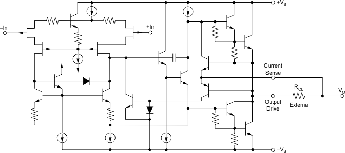
The OPA541 device is a power-operational amplifier capable of operation from power supplies up to
±40 V, and delivering continuous output currents up to 5 A. Internal current-limit circuitry can be user-programmed with a single external resistor, protecting the amplifier and load from fault conditions. The OPA541 devices fabricated are using a proprietary bipolar and FET process.
The OPA541 uses a single current-limit resistor to set both the positive and negative current limits. Applications currently using hybrid power amplifiers requiring two current-limit resistors do need not to be modified.
The OPA541 is available in an 11-pin power plastic package and an industry-standard 8-pin TO-3 hermetic package. The power plastic pachage has a copper-lead frame to maximize heat transfer. The TO-3 package is isolated from all circuitry, allowing it to be mounted directly to a heat sink without special insulators.
PART NUMBER | PACKAGE | BODY SIZE (NOM) |
---|---|---|
OPA541 | TO-220 (11) | 10.70 mm × 20.02 mm |
Changes from A Revision (August 2006) to B Revision
PIN | I/O | DESCRIPTION | |
---|---|---|---|
NO. | NAME | ||
1 | +In | I | +Input |
2 | –In | I | -Input |
3 | –Vs | – | Negative power supply |
4 | –Vs | – | Negative power supply |
5 | Output | O | Output |
6 | NC | – | No internal connection |
7 | Output | O | Output |
8 | Current Sense | I | Current sensing input pin |
9 | NC | – | No internal connection |
10 | +Vs | – | Positive power supply |
11 | +Vs | – | Positive power supply |
MIN | MAX | UNIT | ||
---|---|---|---|---|
Supply voltage, +VS to –VS | 80 | V | ||
Output current | See SOA, Figure 11 | |||
Power dissipation, Internal(2) | 125 | W | ||
Input voltage, differential | +VS | |||
Input voltage, common-mode | +VS | |||
Temperature, pin solder, 10 s | 300 | °C | ||
Junction temperature(2) | 150 | °C | ||
Operating temperature (case) | AP | –40 | 85 | °C |
AM, BM, SM | –55 | 125 | ||
AP | –25 | 85 | ||
Storage temperature, Tstg | AM, BM, SM | –65 | 150 | °C |
VALUE | UNIT | |||
---|---|---|---|---|
V(ESD) | Electrostatic discharge | Human-body model (HBM), per ANSI/ESDA/JEDEC JS-001(1) | ±2000 | V |
Charged-device model (CDM), per JEDEC specification JESD22-C101(2) | ±250 |
MIN | MAX | UNIT | ||
---|---|---|---|---|
Supply Voltage (V+ – V–) | 10 (±5) | 80 (±40) | V | |
Specified temperature | –40 | 125 | °C |
THERMAL METRIC(1) | OPA541 | UNIT | ||
---|---|---|---|---|
KV (TO-220) | LMF (TO-3) | |||
11 PINS | 8 PINS | |||
RθJA | Junction-to-ambient thermal resistance | 21.5 | — | °C/W |
RθJC(top) | Junction-to-case (top) thermal resistance | 17.4 | — | °C/W |
RθJB | Junction-to-board thermal resistance | 9.2 | — | °C/W |
ψJT | Junction-to-top characterization parameter | 1.5 | — | °C/W |
ψJB | Junction-to-board characterization parameter | 9.2 | — | °C/W |
RθJC(bot) | Junction-to-case (bottom) thermal resistance | 0.1 | 3 | °C/W |
PARAMETER | TEST CONDITIONS | MIN | TYP | MAX | UNIT | ||
---|---|---|---|---|---|---|---|
INPUT OFFSET VOLTAGE | |||||||
VOS | Input offset voltage | Specified temperature range VS = ±10 V to ±VMAX |
OPA541AM/AP | ±2 | ±10 | mV | |
OPA541BM/SM | ±0.1 | ±1 | |||||
vs temperature | OPA541AM/AP | ±20 | ±40 | µV/°C | |||
OPA541BM/SM | ±15 | ±30 | |||||
vs supply voltage | OPA541AM/AP, OPA541BM/SM |
±2.5 | ±10 | µV/V | |||
vs power | ±20 | ±60 | µV/W | ||||
IB | Input bias current | 4 | 50 | pA | |||
IOS | Input offset current | ±1 | ±30 | pA | |||
Specified temperature range | 5 | nA | |||||
INPUT CHARACTERISTICS | |||||||
Common-mode voltage range | Specified temperature range | ±(|VS| – 6) | ±(|VS| – 3) | V | |||
Common-mode rejection | VCM = (|±VS| – 6 V) | 95 | 113 | dB | |||
Input capacitance | 5 | pF | |||||
Input impedance, DC | 1 | TΩ | |||||
GAIN CHARACTERISTICS | |||||||
Open-loop gain at 10 Hz | RL = 6 Ω | 90 | 97 | dB | |||
Gain-bandwidth product | 1.6 | MHz | |||||
OUTPUT | |||||||
Voltage swing | IO = 5 A, continuous | ±(|VS| – 5.5) | ±(|VS| – 4.5) | V | |||
IO = 2 A | ±(|VS| – 4.5) | ±(|VS| – 3.6) | |||||
IO = 0.5 A | ±(|VS| – 4) | ±(|VS| – 3.2) | |||||
Peak current | 9 | 10 | A | ||||
AC PERFORMANCE | |||||||
Slew rate | 6 | 10 | V/µs | ||||
Power bandwidth | RL = 8 Ω, VO = 20 Vrms | 45 | 55 | kHz | |||
Settling time to 0.1% | 2-V Step | 2 | µs | ||||
Capacitive load | Specified temperature range, G = 1 | 3.3 | nF | ||||
Specified temperature range, G > 10 | SOA(1) | ||||||
Phase margin | Specified temperature range, RL = 8 Ω | 40 | °C | ||||
±VS | Power supply voltage | Specified temperature range | ±10 | ±30 | ±35 | V | |
Quiescent current | 20 | 25 | mA | ||||
TCASE | Temperature range | AM, BM, AP | –25 | 85 | °C | ||
OPA541BM/SM | –55 | 125 |