SBAS452A September 2008 – January 2016 PCM3168A
PRODUCTION DATA.
- 1 Features
- 2 Applications
- 3 Description
- 4 Revision History
- 5 Description (continued)
- 6 Device Comparison Table
- 7 Pin Configuration and Functions
-
8 Specifications
- 8.1 Absolute Maximum Ratings
- 8.2 ESD Ratings
- 8.3 Recommended Operating Conditions
- 8.4 Thermal Information
- 8.5 Electrical Characteristics
- 8.6 Timing Requirements: System Clock
- 8.7 Timing Requirements: Power-On Reset
- 8.8 Timing Requirements: Audio Interface for Left-Justified, Right-Justified, and I2S (Slave Mode)
- 8.9 Timing Requirements: Audio Interface for Left-Justified, Right-Justified, and I2S (Master Mode)
- 8.10 Timing Requirements: Audio Interface for DSP and TDM (Slave Mode)
- 8.11 Timing Requirements: Audio Interface for DSP and TDM (Master Mode)
- 8.12 Timing Requirements: DAC Outputs and ADC Outputs
- 8.13 Timing Requirements: Four-Wire Serial Control Interface
- 8.14 Timing Requirements: SCL and SDA Control Interface
- 8.15 Typical Characteristics
-
9 Detailed Description
- 9.1 Overview
- 9.2 Functional Block Diagram
- 9.3
Feature Description
- 9.3.1 Analog Inputs
- 9.3.2 Analog Outputs
- 9.3.3 Voltage References
- 9.3.4 System Clock Input
- 9.3.5 Sampling Mode
- 9.3.6 Reset Operation
- 9.3.7 Highpass Filter (HPF)
- 9.3.8 Overflow Flag
- 9.3.9 Zero Flag
- 9.3.10 Four-Wire (SPI) Serial Control
- 9.3.11 Control Data Word Format
- 9.3.12 Register Write Operation
- 9.3.13 Register Read Operation
- 9.3.14 Two-Wire (I2C) Serial Control
- 9.3.15 Packet Protocol
- 9.3.16 Write Operation
- 9.3.17 Read Operation
- 9.4 Device Functional Modes
- 9.5 Register Maps
- 10Application and Implementation
- 11Power Supply Recommendations
-
12Layout
- 12.1
Layout Guidelines
- 12.1.1 Power-Supply Pins (VCCAD1/2, VCCDA1/2, and VDD1/2)
- 12.1.2 Grounding (AGNDAD1/2, AGNDDA1/2, and DGND1/2)
- 12.1.3 VIN1±, VIN2±, VIN3±, VIN4±, VIN5±, and VIN6± Pins
- 12.1.4 VCOMAD and VCOMDA Pins
- 12.1.5 VREFAD1/2 Pins
- 12.1.6 VOUT1±, VOU2±, VOUT3±, VOUT4±, VOUT5±, VOUT6±, VOUT7±, and VOUT8± Pins
- 12.1.7 MODE Pin
- 12.1.8 RST Pin
- 12.1.9 OVF Pin
- 12.1.10 System Clock and Audio Interface Clocks
- 12.1.11 PowerPAD
- 12.1.12 External Mute Control
- 12.2 Layout Example
- 12.1
Layout Guidelines
- 13Device and Documentation Support
- 14Mechanical, Packaging, and Orderable Information
Package Options
Mechanical Data (Package|Pins)
- PAP|64
Thermal pad, mechanical data (Package|Pins)
- PAP|64
Orderable Information
1 Features
- 24-Bit ΔΣ ADC and DAC
- Six-ChanneL ADC:
- High Performance: Differential and Single-Ended, fS = 48 kHz
- THD+N: –93 dB (Differential and Single-Ended)
- SNR: 107 dB (Differential),
104 dB (Single-Ended) - Dynamic Range: 107 dB (Differential),
104 dB (Single-Ended) - Sampling Rate: 8 kHz to 96 kHz
- System Clock: 256 fS, 384 fS, 512 fS, 768 fS
- Differential Voltage Input: 2 VRMS
- Single-Ended Voltage Input: 1 VRMS
- Decimation Filter:
- Passband Ripple: ±0.035 dB
- Stop Band Attenuation: –75 dB
- On-Chip, Highpass Filter:
0.96 Hz at fS = 48 kHz - Overflow Flag
- Eight-Channel DAC:
- High Performance: Differential, fS = 48 kHz
- THD+N: –94 dB
- SNR: 112 dB
- Dynamic Range: 112 dB
- Sampling Rate: 8 kHz to 192 kHz
- System Clock: 128 fS, 192 fS, 256 fS, 384 fS, 512 fS, 768 fS
- Differential Voltage Output: 8 VPP
- Analog Lowpass Filter Included
- 4x/8x Oversampling Digital Filter:
- Passband Ripple: ±0.0018 dB
- Stop Band Attenuation: –75 dB
- Zero Flag
- Flexible Mode Control:
- Four-Wire SPI™, Two-Wire I2C™ Compatible Serial Control Interface or Hardware Control
- Multi Functions Through SPI or I2C I/F:
- Audio I/F Mode and Format Select for ADC and DAC
- Digital Attenuation and Soft Mute for ADC and DAC
- Digital De-Emphasis: 32, 44.1, and 48 kHz for DAC
- Multi Functions Through H/W Control:
- Audio I/F Mode/Format Select
- Digital De-Emphasis Filter: 44.1 kHz for DAC
- External Reset Pin:
- ADC/DAC Simultaneous
- Audio Interface Mode:
- ADC/DAC Independent Master and Slave
- Audio Data Format:
- ADC/DAC Independent I2S™, Left-Justified, Right-Justified, DSP, TDM
- Power Supplies: 5 V for Analog and 3.3 V for Digital
- Package: HTQFP-64
- Operating Temperature Range:
- Consumer Grade: –40°C to 85°C
- Automotive Audio Grade: –40°C to 105°C
2 Applications
- Car Audio External Amplifiers
- Car Audio AVN Applications
- Home Theaters
- AV Receivers
3 Description
The PCM3168A device is a high-performance, single-chip, 24-bit, 6-in/8-out, audio coder and decoder (codecs) with single-ended and differential-selectable analog inputs and differential outputs.
Device Information(1)
| PART NUMBER | PACKAGE | BODY SIZE (NOM) |
|---|---|---|
| PCM3168A | HTQFP (64) | 10.00 mm x 10.00 mm |
- For all available packages, see the orderable addendum at the end of the data sheet.
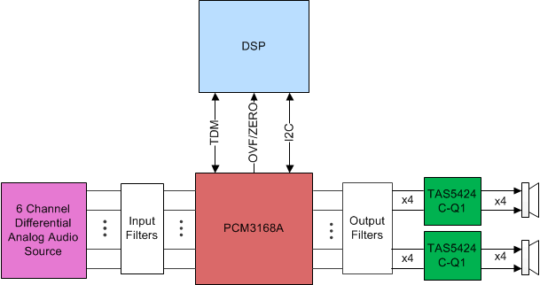
Simplified Application Diagram

4 Revision History
Changes from * Revision (September 2008) to A Revision
- Added ESD Ratings table, Feature Description section, Device Functional Modes section, Application and Implementation section, Power Supply Recommendations section, Layout section, Device and Documentation Support section, and Mechanical, Packaging, and Orderable Information section. Go