SLOS913A October 2015 – February 2017 SN55HVD75-EP
PRODUCTION DATA.
- 1 Features
- 2 Applications
- 3 Description
- 4 Revision History
- 5 Pin Configuration and Functions
- 6 Specifications
- 7 Parameter Measurement Information
- 8 Detailed Description
- 9 Application and Implementation
- 10Power Supply Recommendations
- 11Layout
- 12Device and Documentation Support
- 13Mechanical, Packaging, and Orderable Information
Package Options
Mechanical Data (Package|Pins)
- DRB|8
Thermal pad, mechanical data (Package|Pins)
- DRB|8
Orderable Information
1 Features
- Bus I/O Protection
- >±15-kV HBM Protection
- >±12-kV IEC 61000-4-2 Contact Discharge
- >±4-kV IEC 61000-4-4 Fast Transient Burst
- Extended Industrial Temperature Range
–55°C to 125°C - Large Receiver Hysteresis (80 mV) for Noise Rejection
- Low-Unit-Loading Allows Over 200 Connected Nodes
- Low-Power Consumption
- Low-Standby Supply Current: < 2 µA
- ICC < 1-mA Quiescent During Operation
- 5-V Tolerant Logic Inputs Compatible With
3.3-V or 5-V Controllers - Signaling Rate Options Optimized for:
250 kbps, 20 Mbps, 50 Mbps - Available in a Small VSON Package
-
Supports Defense, Aerospace, and Medical Applications:
- Controlled Baseline
- One Assembly/Test Site
- One Fabrication Site
- Available in Extended (–55°C to 125°C) Temperature Range
- Extended Product Life Cycle
- Extended Product-Change Notification
- Product Traceability
2 Applications
- Factory Automation
- Telecommunications Infrastructure
- Motion Control
3 Description
These devices have robust 3.3-V drivers and receivers in a small package for demanding industrial applications. The bus pins are robust to ESD events with high levels of protection to human-body model and IEC contact discharge specifications.
Each of these devices combines a differential driver and a differential receiver which operate from a single 3.3-V power supply. The driver differential outputs and the receiver differential inputs are connected internally to form a bus port suitable for half-duplex (two-wire bus) communication. These devices feature a wide common-mode voltage range making the devices suitable for multi-point applications over long cable runs. These devices are characterized from –55°C to 125°C.
Device Information(1)
| PART NUMBER | PACKAGE | BODY SIZE (NOM) |
|---|---|---|
| SN55HVD75-EP | VSON (8) | 3.00 mm × 3.00 mm |
- For all available packages, see the orderable addendum at the end of the data sheet.
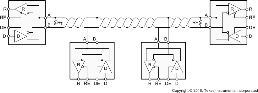
Typical Application Diagram
