SLLS396G SEPTEMBER 1999 – December 2015 SN65LVDS104 , SN65LVDS105
PRODUCTION DATA.
- 1 Features
- 2 Applications
- 3 Description
- 4 Revision History
- 5 Selection Guide to LVDS Repeaters
- 6 Pin Configuration and Functions
-
7 Specifications
- 7.1 Absolute Maximum Ratings
- 7.2 ESD Ratings—JEDEC
- 7.3 ESD Ratings—MIL-STD
- 7.4 Recommended Operating Conditions
- 7.5 Thermal Information
- 7.6 SN65LVDS104 Electrical Characteristics
- 7.7 SN65LVDS105 Electrical Characteristics
- 7.8 SN65LVDS104 Switching Characteristics
- 7.9 SN65LVDS105 Switching Characteristics
- 7.10 Dissipation Ratings
- 7.11 Typical Characteristics
- 8 Parameter Measurement Information
- 9 Detailed Description
-
10Application and Implementation
- 10.1 Application Information
- 10.2
Typical Application
- 10.2.1 Point-to-Point Communications
- 10.2.2 Design Requirements
- 10.2.3
Detailed Design Procedure
- 10.2.3.1 Bypass Capacitance
- 10.2.3.2 Driver Supply Voltage
- 10.2.3.3 Driver Input Voltage
- 10.2.3.4 Driver Output Voltage
- 10.2.3.5 Interconnecting Media
- 10.2.3.6 PCB Transmission Lines
- 10.2.3.7 Termination Resistor
- 10.2.3.8 Receiver Supply Voltage
- 10.2.3.9 Receiver Input Common-Mode Range
- 10.2.3.10 Receiver Input Signal
- 10.2.3.11 Receiver Output Signal
- 10.2.4 Application Curve
- 10.3 Multidrop Communications
- 11Power Supply Recommendations
- 12Layout
- 13Device and Documentation Support
- 14Mechanical, Packaging, and Orderable Information
Package Options
Refer to the PDF data sheet for device specific package drawings
Mechanical Data (Package|Pins)
- PW|16
- D|16
Thermal pad, mechanical data (Package|Pins)
Orderable Information
1 Features
- Receiver and Drivers Meet or Exceed the Requirements of ANSI EIA/TIA-644 Standard
- Typical Data Signaling Rates to 400 Mbps or Clock Frequencies to 400 MHz
- Operates From a Single 3.3-V Supply
- Low-Voltage Differential Signaling With Typical Output Voltage of 350 mV and a 100-Ω Load
- Propagation Delay Time
- SN65LVDS105 – 2.2 ns (Typ)
- SN65LVDS104 – 3.1 ns (Typ)
- LVTTL Levels Are 5-V Tolerant
- Electrically Compatible With LVDS, PECL, LVPECL, LVTTL, LVCMOS, GTL, BTL, CTT, SSTL, or HSTL Outputs With External Networks
- Driver Outputs Are High-Impedance When Disabled or With VCC <1.5 V
- Bus-Pin ESD Protection Exceeds 16 kV
- SOIC and TSSOP Packaging
2 Applications
- Clock Distribution
- Wireless Base Stations
- Network Routers
3 Description
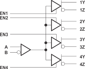
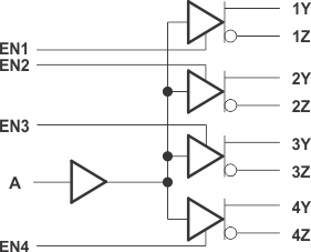
The SN65LVDS10x are a differential line receiver and a LVTTL input (respectively) connected to four differential line drivers that implement the electrical characteristics of low-voltage differential signaling (LVDS). LVDS, as specified in EIA/TIA-644 is a data signaling technique that offers low-power, low-noise coupling, and switching speeds to transmit data at relatively long distances. (Note: The ultimate rate and distance of data transfer is dependent upon the attenuation characteristics of the media, the noise coupling to the environment, and other system characteristics.)
The intended application of this device and signaling technique is for point-to-point baseband data transmission over controlled impedance media of approximately 100 Ω. The transmission media may be printed-circuit board traces, backplanes, or cables. Having the drivers integrated into the same substrate, along with the low pulse skew of balanced signaling, allows extremely precise timing alignment of the signals repeated from the input. This is particularly advantageous in distribution or expansion of signals such as clock or serial data stream.
The SN65LVDS10x are characterized for operation from –40°C to 85°C.
The SN65LVDS10x are members of a family of LVDS repeaters. A brief overview of the family is provided in the Selection Guide to LVDS Repeaters section.
Device Information(1)
| PART NUMBER | PACKAGE | BODY SIZE (NOM) |
|---|---|---|
| SN65LVDS104, SN65LVDS105 | SOIC (16) | 9.90 mm × 3.91 mm |
| TSSOP (16) | 5.00 mm × 4.40 mm |
- For all available packages, see the orderable addendum at the end of the data sheet.
SN65LVDS104 Logic Diagram (Positive Logic)

SN65LVDS105 Logic Diagram (Positive Logic)
