-
SNx400, SNx4LS00, and SNx4S00 Quadruple 2-Input Positive-NAND Gates
- 1 Features
- 2 Applications
- 3 Description
- 4 Revision History
- 5 Pin Configuration and Functions
-
6 Specifications
- 6.1 Absolute Maximum Ratings
- 6.2 ESD Ratings: SN74LS00
- 6.3 Recommended Operating Conditions
- 6.4 Thermal Information
- 6.5 Electrical Characteristics: SNx400
- 6.6 Electrical Characteristics: SNx4LS00
- 6.7 Electrical Characteristics: SNx4S00
- 6.8 Switching Characteristics: SNx400
- 6.9 Switching Characteristics: SNx4LS00
- 6.10 Switching Characteristics: SNx4S00
- 6.11 Typical Characteristics
- 7 Parameter Measurement Information
- 8 Detailed Description
- 9 Application and Implementation
- 10Power Supply Recommendations
- 11Layout
- 12Device and Documentation Support
- 13Mechanical, Packaging, and Orderable Information
- IMPORTANT NOTICE
Package Options
Refer to the PDF data sheet for device specific package drawings
Mechanical Data (Package|Pins)
- D|14
- N|14
Thermal pad, mechanical data (Package|Pins)
Orderable Information
DATA SHEET
SNx400, SNx4LS00, and SNx4S00 Quadruple 2-Input Positive-NAND Gates
1 Features
- Package Options Include:
- Plastic Small-Outline (D, NS, PS)
- Shrink Small-Outline (DB)
- Ceramic Flat (W)
- Ceramic Chip Carriers (FK)
- Standard Plastic (N)
- Ceramic (J)
- Also Available as Dual 2-Input Positive-NAND Gate in Small-Outline (PS) Package
- Inputs Are TTL Compliant; VIH = 2 V and
VIL = 0.8 V - Inputs Can Accept 3.3-V or 2.5-V Logic Inputs
- SN5400, SN54LS00, and SN54S00 are Characterized For Operation Over the Full Military Temperature Range of –55ºC to 125ºC
2 Applications
- AV Receivers
- Portable Audio Docks
- Blu-Ray Players
- Home Theater
- MP3 Players or Recorders
- Personal Digital Assistants (PDAs)
3 Description
The SNx4xx00 devices contain four independent,
2-input NAND gates. The devices perform the Boolean function Y = A .B or Y = A + B in positive logic.
Device Information(1)
| PART NUMBER | PACKAGE | BODY SIZE (NOM) |
|---|---|---|
| SN74LS00DB | SSOP (14) | 6.20 mm × 5.30 mm |
| SN7400D, SN74LS00D, SN74S00D | SOIC (14) | 8.65 mm × 3.91 mm |
| SN74LS00NSR | PDIP (14) | 19.30 × 6.35 mm |
| SNJ5400J, SNJ54LS00J, SNJ54S00J | CDIP (14) | 19.56 mm × 6.67 mm |
| SNJ5400W, SNJ54LS00W, SNJ54S00W | CFP (14) | 9.21 mm × 5.97 mm |
| SN54LS00FK, SN54S00FK | LCCC (20) | 8.89 mm × 8.89 mm |
| SN7400NS, SN74LS00NS, SN74S00NS | SO (14) | 10.30 mm × 5.30 mm |
| SN7400PS, SN74LS00PS | SO (8) | 6.20 mm × 5.30 mm |
- For all available packages, see the orderable addendum at the end of the data sheet.
Logic Diagram, Each Gate (Positive Logic)

4 Revision History
Changes from C Revision (November 2016) to D Revision
- Changed Typical Application Diagram see Application and Implementation section.Go
Changes from B Revision (October 2003) to C Revision
- Added ESD Ratings table, Feature Description section, Device Functional Modes, Application and Implementation Power Supply Recommendations section, Layout section, Device and Documentation Support section, and Mechanical, Packaging, and Orderable Information section.Go
- Changed Ordering Information table to Device Comparison Table; see Package Option Addendum at the end of the data sheetGo
- Changed Package thermal impedance, RθJA, values in Thermal Information table From: 86°C/W To: 90.9°C/W (D), From: 96°C/W To: 102.8°C/W (DB), From: 80°C/W To: 54.8°C/W (N), and From: 76°C/W To: 89.7°C/W (NS)Go
5 Pin Configuration and Functions
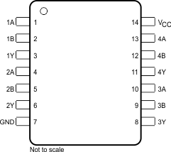
SN5400 J, SN54xx00 J and W, SN74x00 D, N, and NS, or SN74LS00 D, DB, N, and NS Packages
14-Pin CDIP, CFP, SOIC, PDIP, SO, or SSOP
Top View

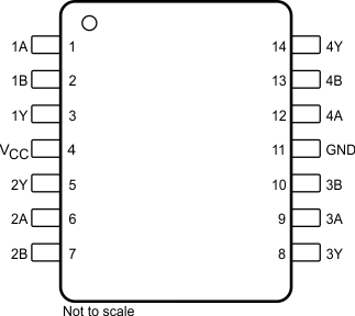
SN5400 W Package
14-Pin CFP
Top View

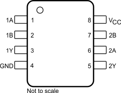
SN74xx00 PS Package
18-Pin SO
Top View

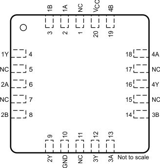
SN54xx00 FK Package
20-Pin LCCC
Top View

Pin Functions
| PIN | I/O | DESCRIPTION | ||||
|---|---|---|---|---|---|---|
| NAME | CDIP, CFP, SOIC, PDIP, SO, SSOP |
SO (SN74xx00) |
CFP (SN5400) |
LCCC | ||
| 1A | 1 | 1 | 1 | 2 | I | Gate 1 input |
| 1B | 2 | 2 | 2 | 3 | I | Gate 1 input |
| 1Y | 3 | 3 | 3 | 4 | O | Gate 1 output |
| 2A | 4 | 6 | 6 | 6 | I | Gate 2 input |
| 2B | 5 | 7 | 7 | 8 | I | Gate 2 input |
| 2Y | 6 | 5 | 5 | 9 | O | Gate 2 output |
| 3A | 10 | — | 9 | 13 | I | Gate 3 input |
| 3B | 9 | — | 10 | 14 | I | Gate 3 input |
| 3Y | 8 | — | 8 | 12 | O | Gate 3 output |
| 4A | 13 | — | 12 | 18 | I | Gate 4 input |
| 4B | 12 | — | 13 | 19 | I | Gate 4 input |
| 4Y | 11 | — | 14 | 16 | O | Gate 4 output |
| GND | 7 | 4 | 11 | 10 | — | Ground |
| NC | — | — | — | 1, 5, 7, 11, 15, 17 |
— | No connect |
| VCC | 14 | 8 | 4 | 20 | — | Power supply |