SCDS168A May 2004 – September 2015 SN74CB3Q16244
PRODUCTION DATA.
- 1 Features
- 2 Applications
- 3 Description
- 4 Revision History
- 5 Description continued
- 6 Pin Configuration and Functions
- 7 Specifications
- 8 Parameter Measurement Information
- 9 Detailed Description
- 10Application and Implementation
- 11Power Supply Recommendations
- 12Layout
- 13Device and Documentation Support
- 14Mechanical, Packaging, and Orderable Information
Package Options
Refer to the PDF data sheet for device specific package drawings
Mechanical Data (Package|Pins)
- DGG|48
- DL|48
- DGV|48
Thermal pad, mechanical data (Package|Pins)
Orderable Information
1 Features
- High-Bandwidth Data Path (Up to 500 MHz)(1)(1)
- 5-V Tolerant I/Os With Device Powered Up or Powered Down
- Low and Flat ON-State Resistance (ron) Characteristics Over Operating Range
(ron= 5 Ω Typical) - Rail-to-Rail Switching on Data I/O Ports
- 0 to 5-V Switching With 3.3-V VCC
- 0 to 3.3-V Switching With 2.5-V VCC
- Bidirectional Data Flow With Near-Zero Propagation Delay
- Low Input and Output Capacitance Minimizes Loading and Signal Distortion
(Cio(OFF) = 4 pF Typical) - Fast Switching Frequency (fOE = 20 MHz Maximum)
- Data and Control Inputs Provide Undershoot Clamp Diodes
- Low Power Consumption (ICC = 1 mA Typical)
- VCC Operating Range From 2.3 V to 3.6 V
- Data I/Os Support 0 to 5-V Signaling Levels
(0.8 V, 1.2 V, 1.5 V, 1.8 V, 2.5 V, 3.3 V, 5 V) - Control Inputs Can Be Driven by TTL or
5-V and 3.3-V CMOS Outputs - Ioff Supports Partial-Power-Down Mode Operation
- Latch-Up Performance Exceeds 100 mA
Per JESD 78, Class II - ESD Performance Tested Per JESD 22
- 2000-V Human Body Model
(A114-B, Class II) - 1000-V Charged-Device Model (C101)
- 2000-V Human Body Model
- Supports Both Digital and Analog Applications (1)
2 Applications
- IP Phones: Wired and Wireless
- Optical Modules
- Optical Networking: Video Over Fiber and EPON
- Private Branch Exchange (PBX)
- WiMAX and Wireless Infrastructure Equipment
3 Description
The SN74CB3Q16244 device is a high-bandwidth FET bus switch using a charge pump to elevate the gate voltage of the pass transistor, providing a low and flat ON-state resistance (ron). The low and flat ON-state resistance allows for minimal propagation delay and supports rail-to-rail switching on the data input/output (I/O) ports. The SN74CB3Q16244 device also features low data I/O capacitance to minimize capacitive loading and signal distortion on the data bus. Specifically designed to support high-bandwidth applications, the SN74CB3Q16244 device provides an optimized interface solution ideally suited for broadband communications, networking, and data-intensive computing systems.
Device Information(1)
| PART NUMBER | PACKAGE | BODY SIZE (NOM) |
|---|---|---|
| SN74CB3Q16244DGG | TSSOP (48) | 12.50 mm × 6.10 mm |
| SN74CB3Q16244DGV | TVSOP (48) | 9.70 mm × 4.40 mm |
| SN74CB3Q16244DL | SSOP (48) | 15.88 mm × 7.49 mm |
- For all available packages, see the orderable addendum at the end of the data sheet.
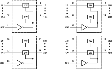
Logic Diagram (Positive Logic)

4 Revision History
Changes from A Revision (March 2005) to B Revision
- Added Applications, Device Information table, Pin Configuration and Functions section, ESD Ratings table, Feature Description section, Device Functional Modes, Application and Implementation section, Power Supply Recommendations section, Layout section, Device and Documentation Support section, and Mechanical, Packaging, and Orderable Information section Go
- Removed Ordering Information table. Go